Method and structure of in-situ wafer scale polymer stud grid array contact formation

a polymer stud and grid array technology, applied in the field of polymer stud grid array contact formation, can solve the problems of many expensive testers and handlers, many sophisticated heated chambers, and many expensive high-temperature printed circuit boards and sockets

Inactive Publication Date: 2002-09-05
SIEMENS DEMATIC
View PDF4 Cites 71 Cited by
  • Summary
  • Abstract
  • Description
  • Claims
  • Application Information

AI Technical Summary

Problems solved by technology

Because testing of individual bare die, or packaged die, requires numerous and costly testers and handlers, which spend a majority of time moving and handling the devices.
In addition, bare IC...

Method used


Image

  • Method and structure of in-situ wafer scale polymer stud grid array contact formation
  • Method and structure of in-situ wafer scale polymer stud grid array contact formation
  • Method and structure of in-situ wafer scale polymer stud grid array contact formation

Examples


Embodiment Construction

[0024] A general process flow description of exemplary embodiments of the present invention will now be given with respect to a semiconductor wafer. Bond pads (typically aluminum, but copper is beginning to be more common) formed on the wafers are coated to prevent high contact resistance and corrosion in subsequent fabrication steps, environmental testing, or in application environments. This coating is called pad cover metallurgy (PCM).

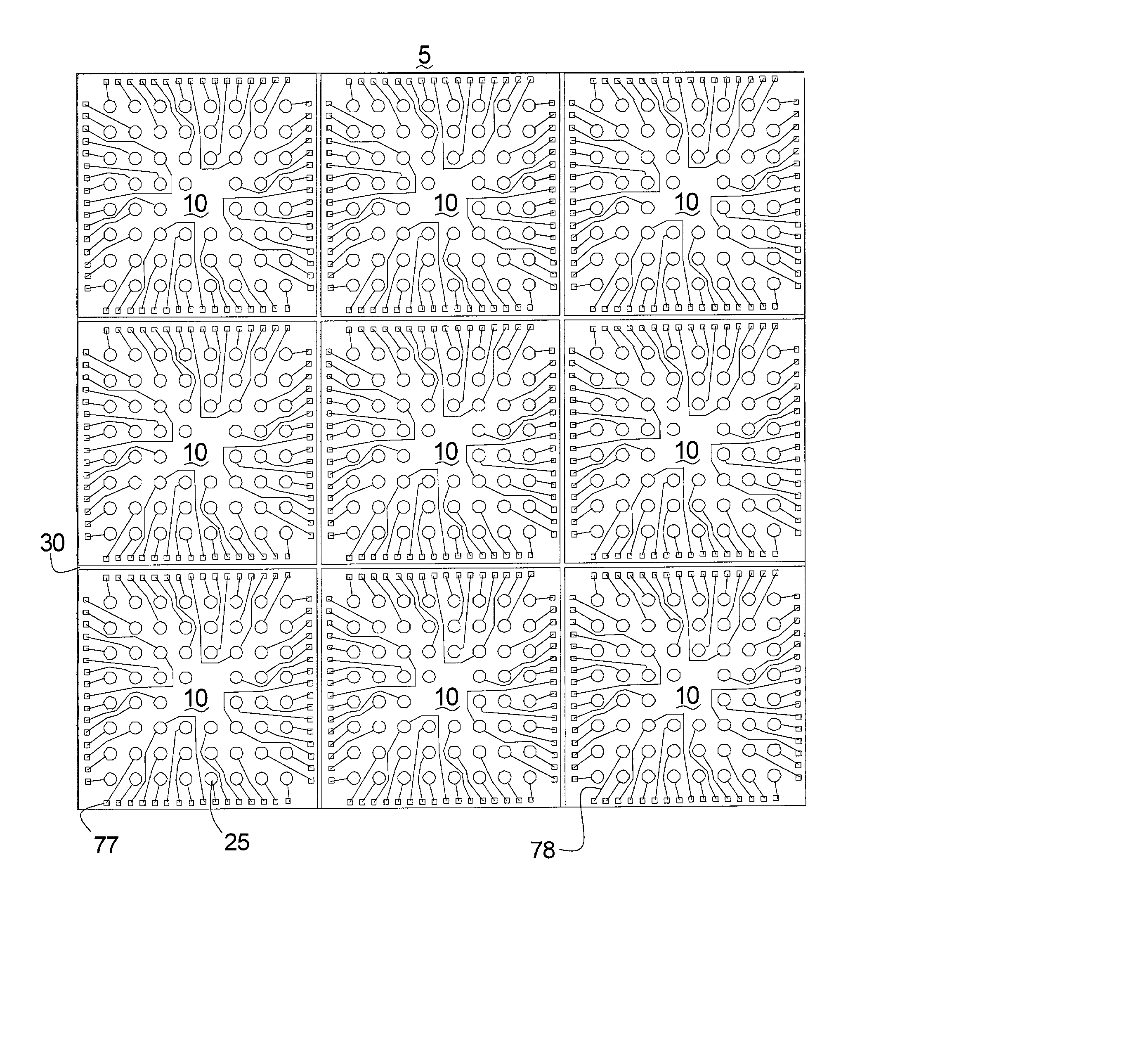
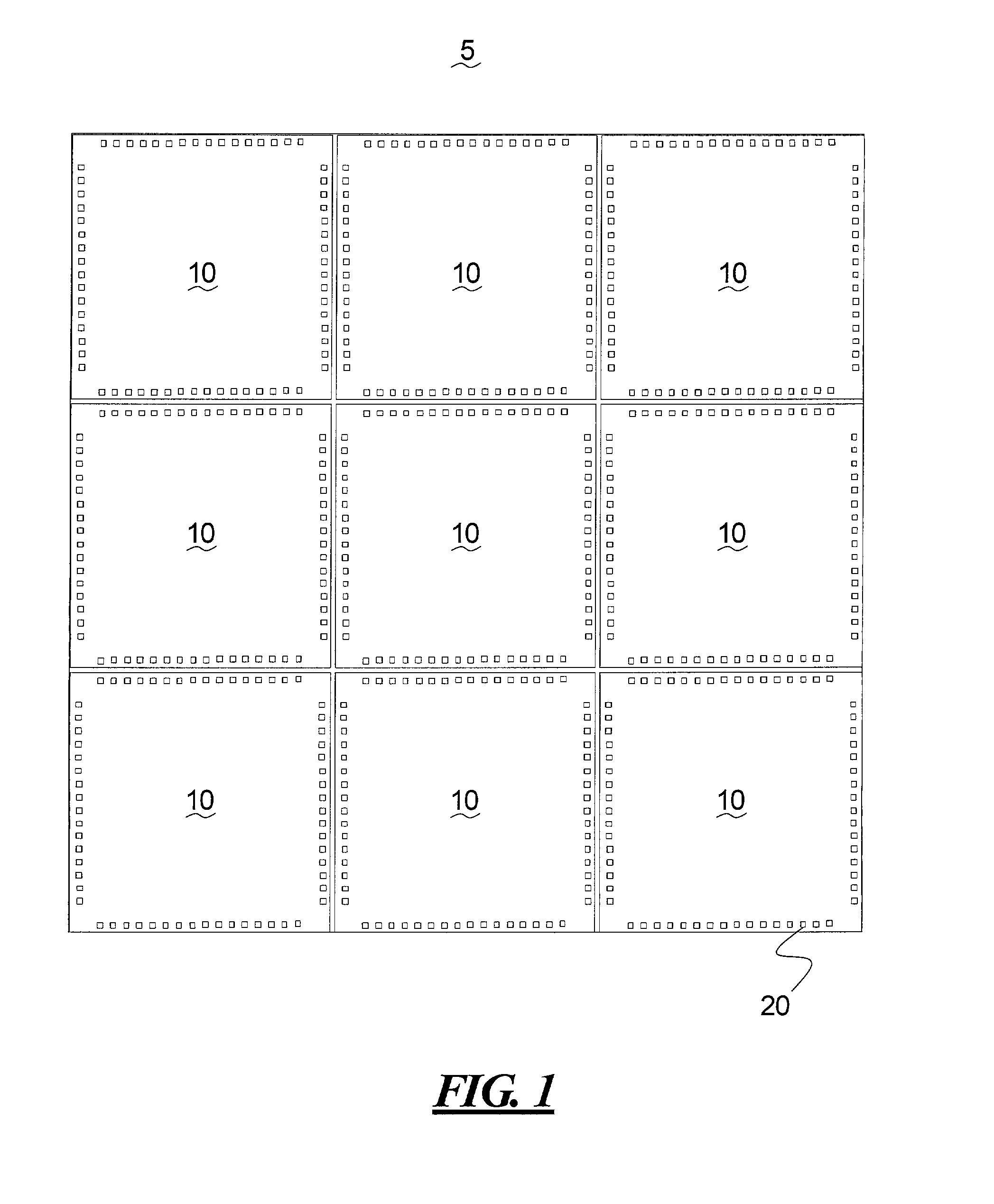
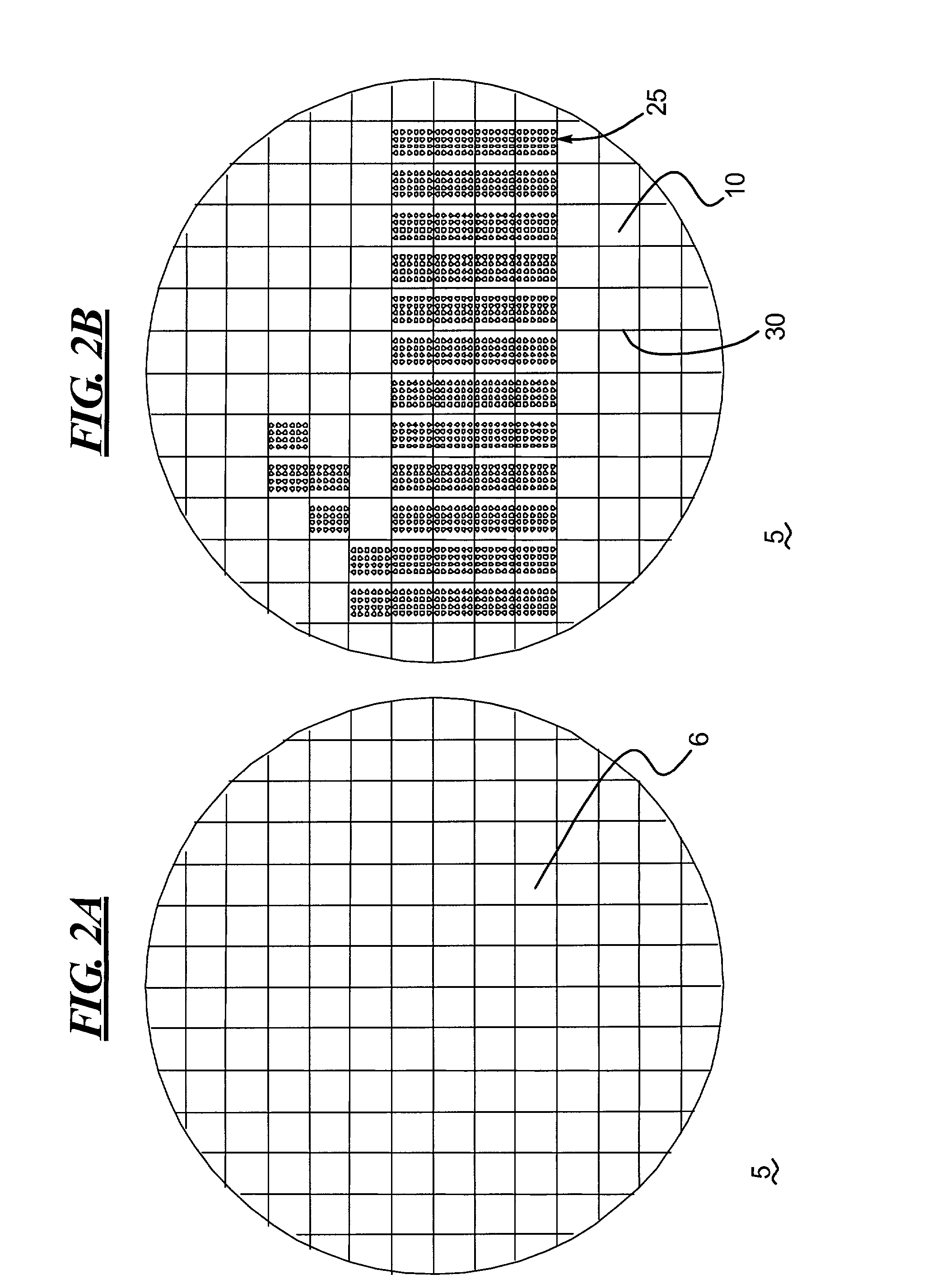
[0025] FIG. 1 shows a detailed plan view of a segment of a region of the IC wafer 5 having nine integrated circuit (IC) devices 10. Each IC device 10 has a perimeter array of coated input / output (I / O) bond pads 20, which are also shown in cross section in FIG. 5. Perimeter bond pad 20 locations are illustrated, but it is within the scope of this invention to include bond pads disposed in any location across the area of IC devices 10.

[0026] The PCM coating 70, shown in cross section in FIG. 5, on the pads 20 may include electroless nickel and gold; t...


PUM


Abstract

Methods and structures of in-situ wafer scale polymer stud grid array (ISWS-PSGA) contact formation on integrated circuit devices, wherein a separate pre-manufactured PSGA substrate is not needed. The methods include injection molding of thermoplastics, transfer-molding of thermoset materials, lamination of polymer films with subsequent in-situ molding/embossing, and forming the PSGA structure directly on the semiconductor wafer. The ISWS-PSGA structure extends across the entire semiconductor wafer, with ISWS-PSGA metallized input/output studs disposed across each of the integrated circuit devices on the wafer. The polymer formed on the wafer surface to create the stud field is extended beyond the perimeter of the wafer, and the polymer film extension is used for temporary connection to an integrated circuit tester, or an integrated circuit test/burn-in system. The extension may further include studs for contacting the tester.

Description

REFERENCE TO PROVISIONAL APPLICATION[0001] This application claims benefit to U.S. provisional application 60 / 272,520 filed Mar. 1, 2001, which is incorporated herein by reference.[0002] 1. Field of the Invention[0003] The present invention is generally directed to polymer stud grid arrays (PSGAs). In particular the present invention is directed to methods of forming in-situ wafer scale polymer stud grid arrays (ISWS-PSGAs), and structures formed using the methods.[0004] 2. Discussion of the Related Art[0005] Wafer level packaging is in high demand due to miniaturization benefits. Formation of input / output (I / O) features on integrated circuit (IC) devices while still in wafer form is very desirable, since it allows for simpler IC-level testing and lower cost testing. In addition, wafer level packaging is more efficient because it eliminates packaging of each individual IC after wafer dicing. Moreover, the need for "assembly" packaging processes is eliminated.[0006] Wafer level test / ...

Claims


Application Information

Patent Timeline
IPC IPC(8): H01L21/60H01L23/485
CPCH01L24/11H01L2224/13099H01L2924/01003H01L2924/01012H01L2924/01013H01L2924/01022H01L2924/01027H01L2924/01029H01L2924/01046H01L2924/01074H01L2924/01078H01L2924/01079H01L2924/01082H01L2924/01327H01L2924/10329H01L2924/14H01L24/13H01L2924/01006H01L2924/01023H01L2924/01024H01L2924/01033H01L2924/01043H01L2924/014H01L2224/1319H01L2224/13644H01L2224/13655H01L2924/00014H01L2924/0001H01L24/03H01L24/05H01L2224/05001H01L2224/05022H01L2224/05027H01L2224/05184H01L2224/05572H01L2224/06131H01L2924/12042H01L2924/00H01L2224/05647H01L2224/05144H01L2224/05147H01L2224/05155H01L2224/05164H01L2224/05166H01L2224/05171
Inventor HIGGINS, LEO M. III
Owner SIEMENS DEMATIC
Why Eureka
Try Eureka