Pixel structure of an organic light-emitting diode display device and its fabrication method

a technology of light-emitting diodes and display devices, which is applied in the direction of discharge tubes, luminescent screens, identification means, etc., can solve the problems of insufficient brightness and luminous efficiency of oel devices, inability to produce display devices of high resolution, and even worse overall brightness and luminous efficiency. , to achieve the effect of wide viewing angle, high luminous efficiency and high resolution

Inactive Publication Date: 2002-09-12
IND TECH RES INST
View PDF0 Cites 39 Cited by
  • Summary
  • Abstract
  • Description
  • Claims
  • Application Information

AI Technical Summary

Benefits of technology

0008] According to the invention, the pixel structure of the full-color OLED display device uses blue organic light-emitting diodes or polymer light-emitting diodes as the electroluminescent media. The low-temperature poly Si (LTPS) thin film transistors provide a current to the OLED device and serve as an ...

Problems solved by technology

There are some difficulties to overcome in order for the full-color organic electroluminescent display devices to be accepted the market of flat-panel displays.
For instance, it is not easy to produce display devices of high resolution, high luminous efficiency and wide viewing angle.
The brightness and luminous efficiency are not good eno...

Method used


Image

  • Pixel structure of an organic light-emitting diode display device and its fabrication method
  • Pixel structure of an organic light-emitting diode display device and its fabrication method
  • Pixel structure of an organic light-emitting diode display device and its fabrication method

Examples


Embodiment Construction

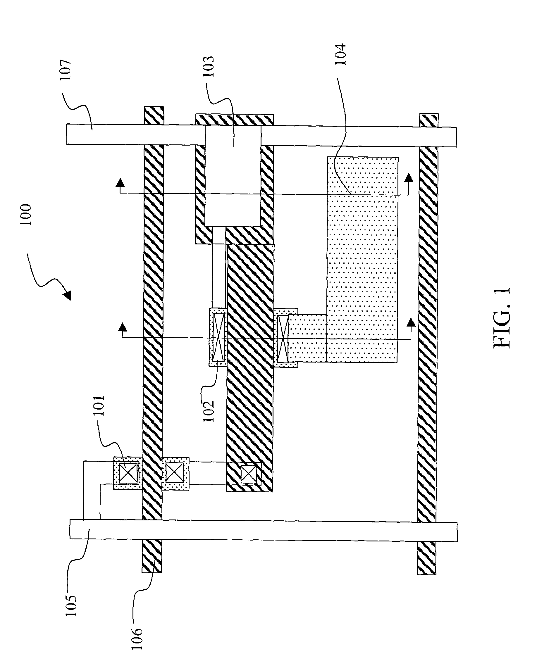
[0021] FIG. 3 is a schematic diagram of a full-color OLED display device according to the invention. Each pixel structure 300 of the full-color OLED display device comprises mainly two thin film transistors T.sub.1 and T.sub.2, a storage capacitor C.sub.s, and an OLED device structure. Both thin film transistors T.sub.1 and T.sub.2 comprise respectively a source electrode, a drain electrode and a gate electrode. The gate electrode of the TFT T.sub.1 comprises a portion of a gate line 301. The source electrode of the TFT T.sub.1 is electrically connected to a data line 302 and the drain electrode is electrically connected to the gate electrode of the TFT T.sub.2. The gate electrode of the TFT T.sub.2 is electrically connected to the storage capacitor C.sub.s. The OLED device structure is electrically connected to the drain electrode of the TFT T.sub.2.

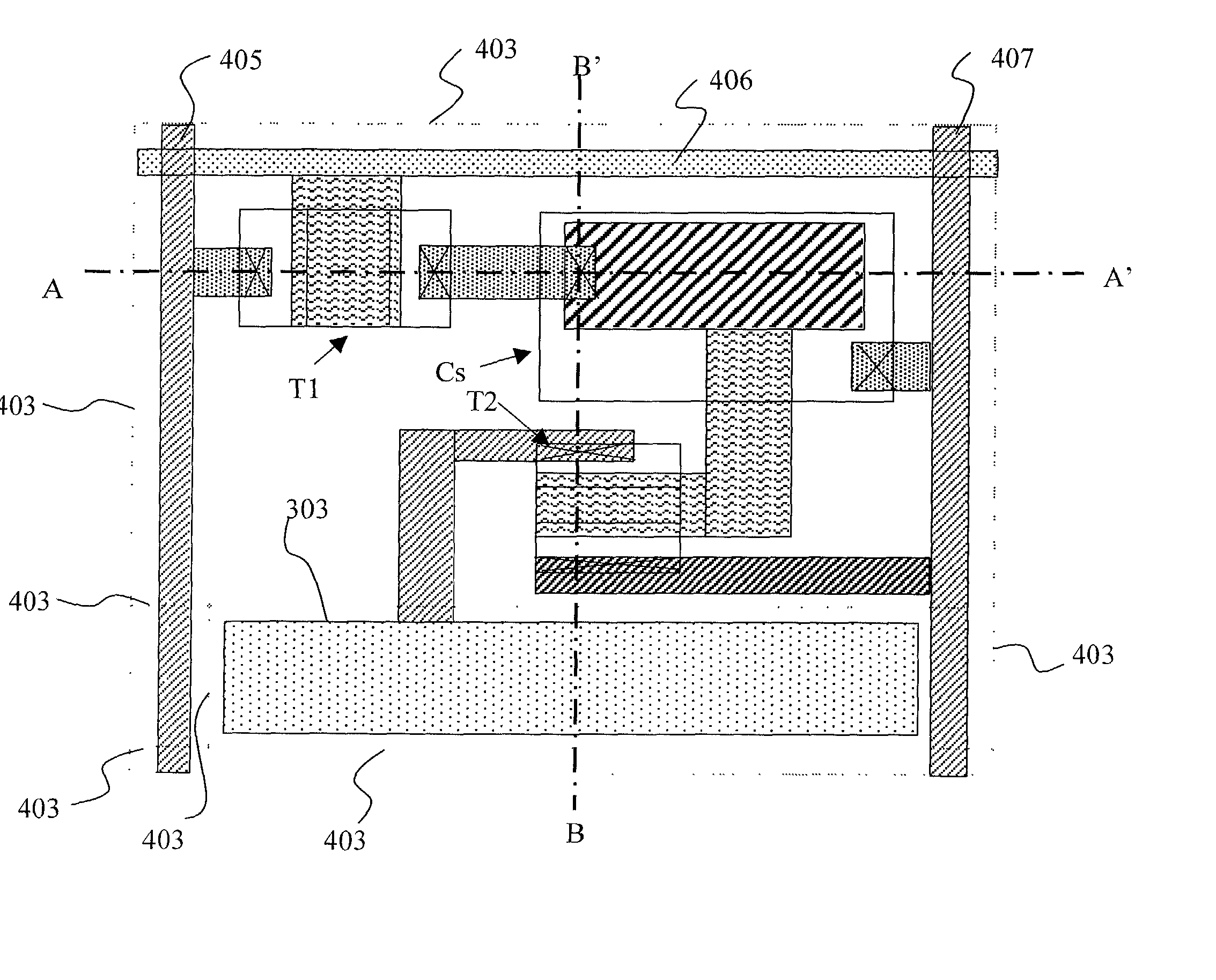
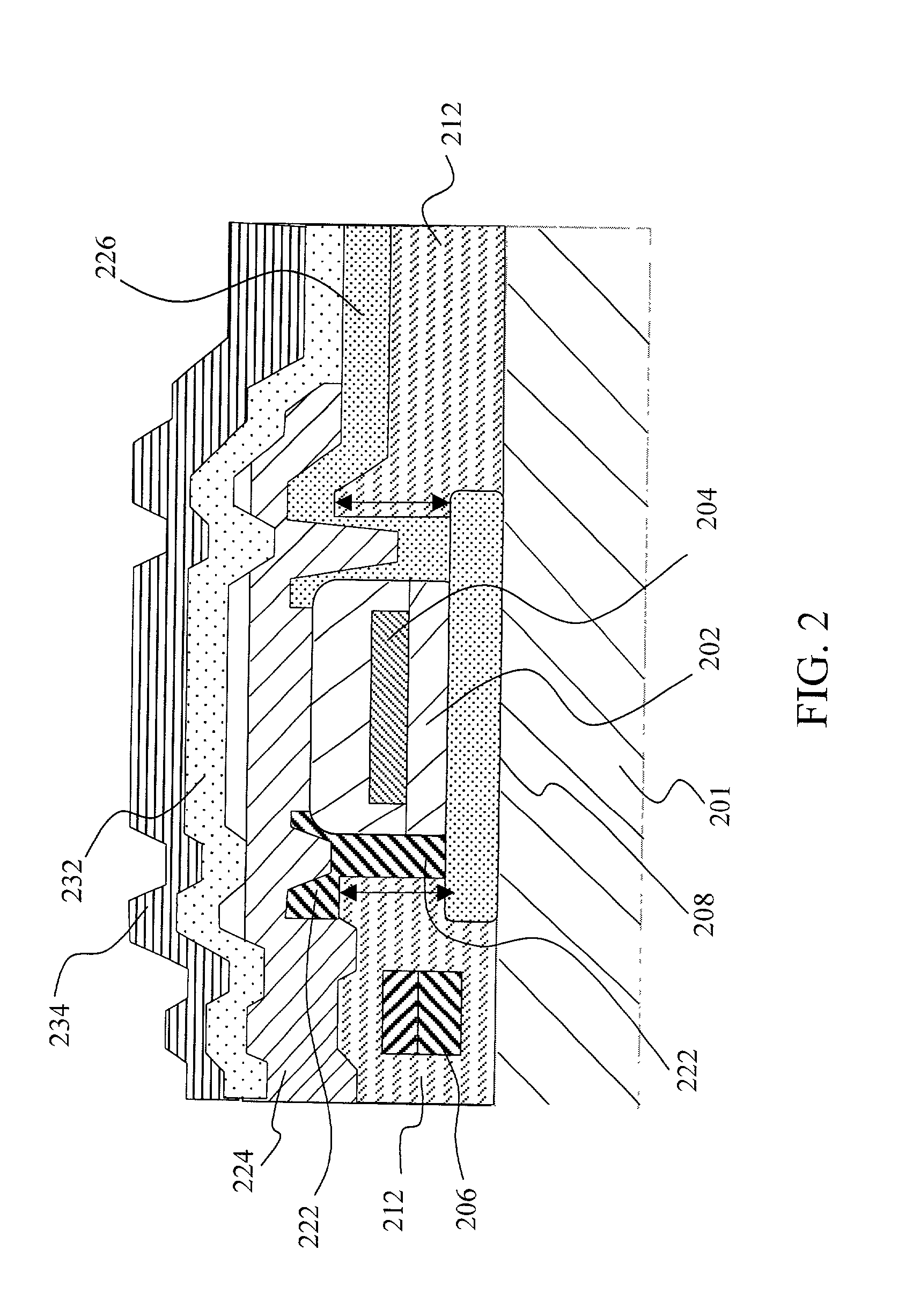
[0022] FIG. 4 is a diagrammatic plan view of a full-color OLED display device according to the invention. Referring to FIG. 4, the TFT...


PUM


Abstract

A pixel structure of a full-color organic light-emitting diode (OLED) display device comprises a black matrix, a color changing medium, two thin film transistors, a storage capacitor, and an OLED device arranged on a substrate. The pixel structure of the display device uses blue organic light-emitting diodes or polymer light-emitting diodes as electroluminescent media. The low-temperature poly Si (LTPS) thin film transistors provide a current to the OLED device and serve as an active driving device. The color changing medium changes blue light into red or green light to form full-color OLED. The processing steps include the black matrix process, the island process, the gate process, the interlayer process, the color changing medium process, and the OLED deposition process. Because a color changing medium is integrated on the LTPS thin film transistors, this invention can make display devices of high resolution, high luminous efficiency and wide viewing angle.

Description

FIELD OF THE INVENTION[0001] The present invention relates generally to a pixel structure of an organic light-emitting diode (OLED) display device and its fabrication method, and more particularly to a pixel structure of a full-color OLED display device and its fabrication method.BACKGROUND OF THE INVENTION[0002] Flat-panel displays have become one of the most important electronic devices in products such as notebook computers and pocket-TVs. Among the flat-panel displays, organic electroluminescent (OEL) displays have the following advantages: light emitting, high luminous efficiency, wide viewing angle, fast response speed, high reliability, full color, low driving voltage, low power consumption and simple fabrication. Undoubtedly, this product has emerged as the display of choice in the market place. The fabrication method of a conventional full-color OLED display device includes at least the following five methods: (a) using a precision photo-mask to get a pixel array of red, gr...

Claims


Application Information

Patent Timeline
IPC IPC(8): G09F9/30H05B33/12H01L21/336H01L27/32H01L29/786H01L51/50H05B33/10
CPCH01L27/322H01L27/3244H01L51/5284H10K59/38H10K59/12H10K50/865
Inventor SHEU, CHAI-YUANWANG, WEN-CHUNYEH, YUNG-HUI
Owner IND TECH RES INST
Why Eureka
Try Eureka