Steady state method for measuring the thickness and the capacitance of ultra thin dielectric in the presence of substantial leakage current

a capacitance measurement and ultra-thin dielectric technology, applied in the field of semi-conductor wafer testing, can solve the problems of significant errors in calculating reduced .q.sub.c, and thin dielectric film thickness, and achieve effective and accurate measurement of the thickness of the dielectric layer

Inactive Publication Date: 2002-09-12
SEMICON DIAGNOSTICS
View PDF0 Cites 44 Cited by
  • Summary
  • Abstract
  • Description
  • Claims
  • Application Information

AI Technical Summary

Benefits of technology

0006] In general, the invention relates to an apparatus and method for producing electrical measurements of capacitance and thickness of ultra-thin dielectric layers on semiconductor substrates (wafers). The apparatus and method produces effective and accurate measurements of the dielectric layer thickness despite substantial leakage of current across the layer and no apriori knowledge of the relationship between the leakage current characteristics, i.e., measured electrical properties such as voltage and current, and thickness of

Problems solved by technology

Due to substantial leakage of current across the dielectric layer, via tunneling, the method described in U.S. Pat. No. 6,037,797 is ineffective for determining the thickness of ultra-thin dielectrics films, i.e. dielectric films having an EOT equal to or less than about 40 .ANG.. When leakage current tunnels through the dielectric layer, the charge .DELTA.Q.sub.C is reduced by the amount of charge transported across a dielectric layer during the time of charging and measuring .DELTA.V. In thicker dielectric layers, such as SiO.sub.2, the leakag

Method used


Image

  • Steady state method for measuring the thickness and the capacitance of ultra thin dielectric in the presence of substantial leakage current
  • Steady state method for measuring the thickness and the capacitance of ultra thin dielectric in the presence of substantial leakage current
  • Steady state method for measuring the thickness and the capacitance of ultra thin dielectric in the presence of substantial leakage current

Examples


Embodiment Construction

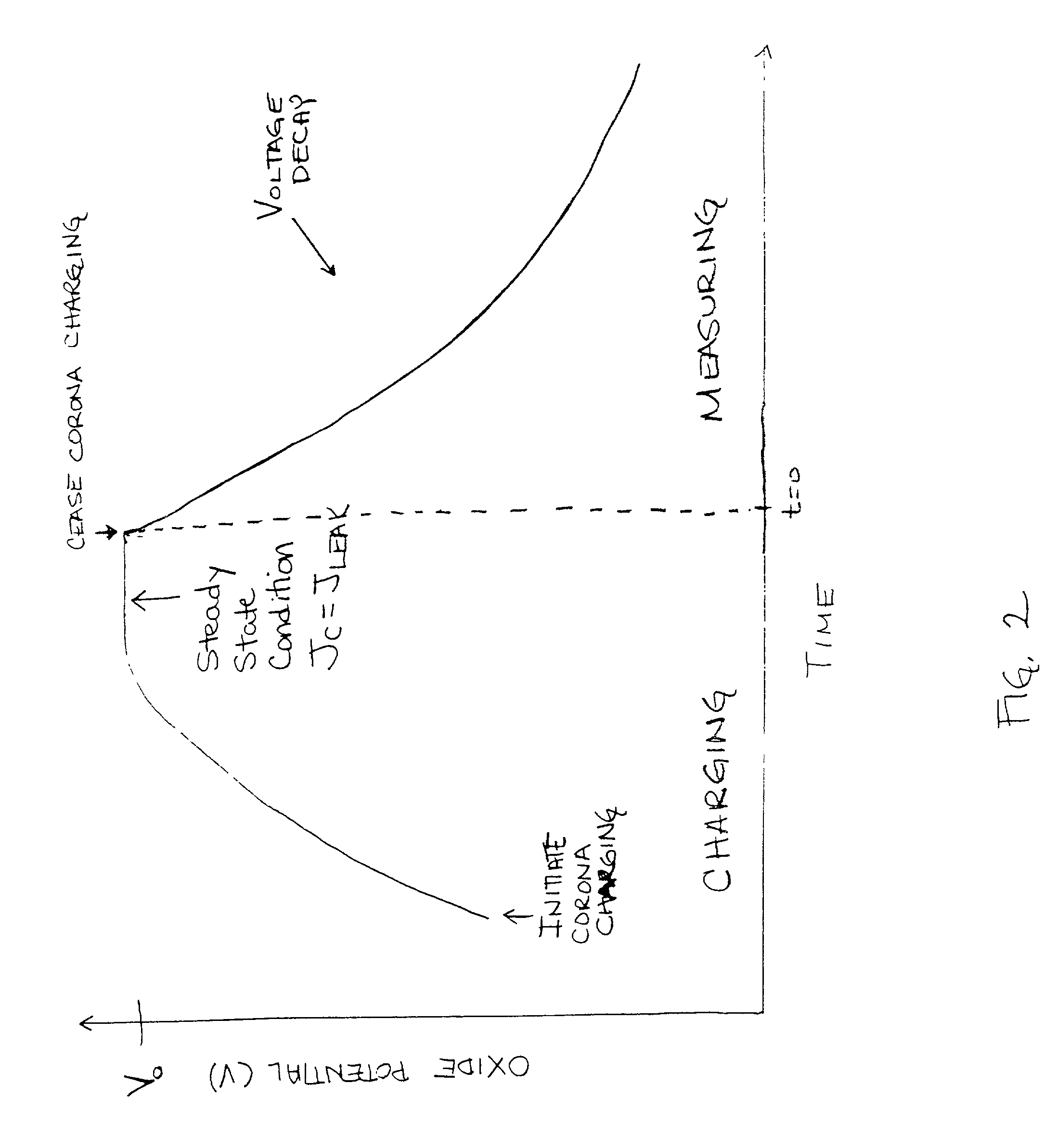
[0023] The methodology for measuring ultra-thin dielectric layer thicknesses includes depositing an electric charge using a corona current, J.sub.C, from a corona discharge source, onto a dielectric layer of a semiconductor wafer to produce a steady state condition in which the leakage current, J.sub.LEAK, equals J.sub.C; terminating the corona current; measuring electrical parameters of the wafer, such as the dielectric potential or the potential decay rate; and

[0024] comparing the measured electrical parameters to calibrated parameters to derive the ultra-thin dielectric thickness.

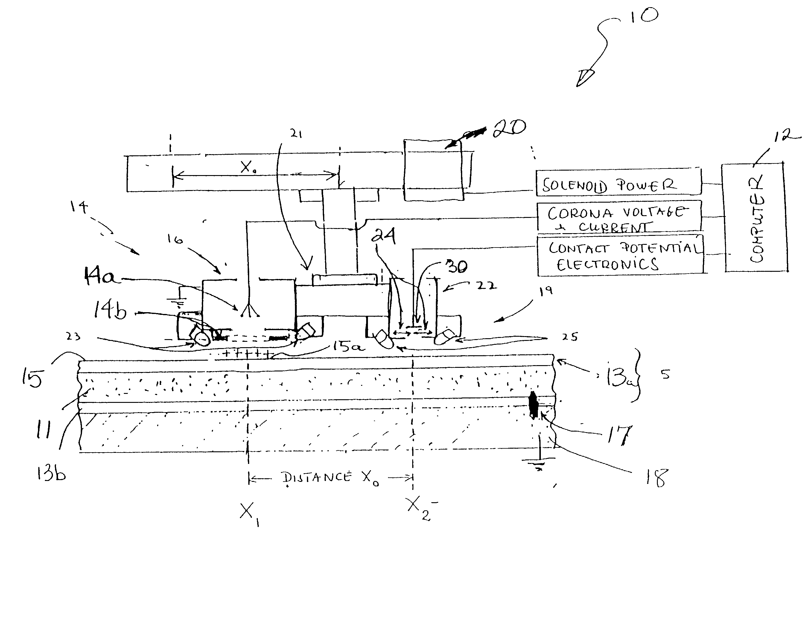
[0025] Referring to FIG. 1, a computer controlled test system 10 is used to measure the oxide thickness of a top dielectric layer 13a placed on a semiconductor wafer 5 on a testing site 15a. An example of the computer controlled test system 10 can be found in U.S. Pat. application Ser. No. 09 / 451,652 by Lagowski et al. which is incorporated herein in its entirety by reference. Semiconducting wafer 5 incl...


PUM


Abstract

A method is described for measuring the capacitance and the equivalent oxide thickness of an ultra thin dielectric layer on a silicon substrate in which the dielectric layer is uniform or patterned. The surface of a dielectric layer is electrically charged by a flux on ions from a corona discharge source until a steady state is reached when the corona flux is balanced by the leakage current across a dielectric. The flux is abruptly terminated and the surface potential of a dielectric is measured versus time. The steady state value of the surface potential is obtained by extrapolation of the potential decay curve to the initial moment of ceasing the corona flux. The thickness of a dielectric layer is determined by using the steady state potential or by using the value of the surface potential after a predetermined time.

Description

CROSS-RELATED APPLICATIONS[0001] This application is a continuation-in-part of application Ser. No. 09 / 810,789, filed Mar. 16, 2001, now pending, and under 35 USC .sctn.119(e)(1), claims the benefit of provisional application Ser. No. 60 / 264,571, filed Jan. 26, 2001.BACKGROUND[0002] The invention relates to semiconductor wafer testing and more particularly to characterizing the thickness and capacitance of a dielectric layer on a semiconductor wafer in the presence of substantial leakage current.[0003] As is known in the art, semiconductor devices often contain dielectric layers (e.g., silicon dioxide) grown / or deposited on a semiconductor substrate (e.g., silicon). Semiconductor wafers including dielectric layers are used in manufacturing microelectronic devices such as metal-oxide-semiconductor (MOS) capacitors, MOS-field effect transistors (MOSFET), and related integrated circuits.[0004] During manufacture of microelectronic devices, the thickness of the dielectric layer must be ...

Claims


Application Information

Patent Timeline
IPC IPC(8): G01R31/26G01R31/302
CPCG01B7/085G01R31/2648
Inventor SAVTCHOUK, ALEXANDERLAGOWSKI, JACEKD'AMICO, JOHNWILSON, MARSHALL D.JASTRZEBSKI, LUBOMIR L.
Owner SEMICON DIAGNOSTICS
Why Eureka
Try Eureka