System and method for measuring a capacitance associated with an integrated circuit

a technology of integrated circuits and capacitance measurements, applied in the field of integrated circuits, can solve the problems of inability to meet the requirements of the intended purpose, poor performance, and significant problems in the system or architecture with precise or exact specifications, and achieve the effects of eliminating capacitance, enhancing the and high accuracy of the capacitance measuremen

Inactive Publication Date: 2005-03-22
TEXAS INSTR INC
View PDF10 Cites 34 Cited by
  • Summary
  • Abstract
  • Description
  • Claims
  • Application Information

AI Technical Summary

Benefits of technology

Certain embodiments of the present invention may provide a number of technical advantages. For example, according to one embodiment of the present invention, a measurement approach is provided that allows highly accurate capacitance measurements to be obtained for a semiconductor as it propagates through the manufacturing process. The enhanced accuracy of the capacitance measurement is a result of the elimination of capacitances between elements or conductors of a device under test. The elimination of their capacitance is achieved by charging and discharging multiple conductors in phase and thus effectively shorting neighboring conductors proximate to a conductor being targeted for the capacitance measurement. Accordingly, the capacitances of associated or neighboring elements that may otherwise act to negatively influence a capacitance measurement are negated or otherwise removed from the measurement equation. The enhanced capacitance measurement provides the opportunity to more closely monitor the manufacture of a semiconductor.
Another technical advantage of one embodiment of the present invention is a result of the isolatio...

Problems solved by technology

Semiconductor characteristics or parameters that vary significantly from their designated values may cause significant problems in systems or architectures with precise or exact specifications.
When system parameters become skewed because of in...

Method used


Image

  • System and method for measuring a capacitance associated with an integrated circuit
  • System and method for measuring a capacitance associated with an integrated circuit
  • System and method for measuring a capacitance associated with an integrated circuit

Examples


Embodiment Construction

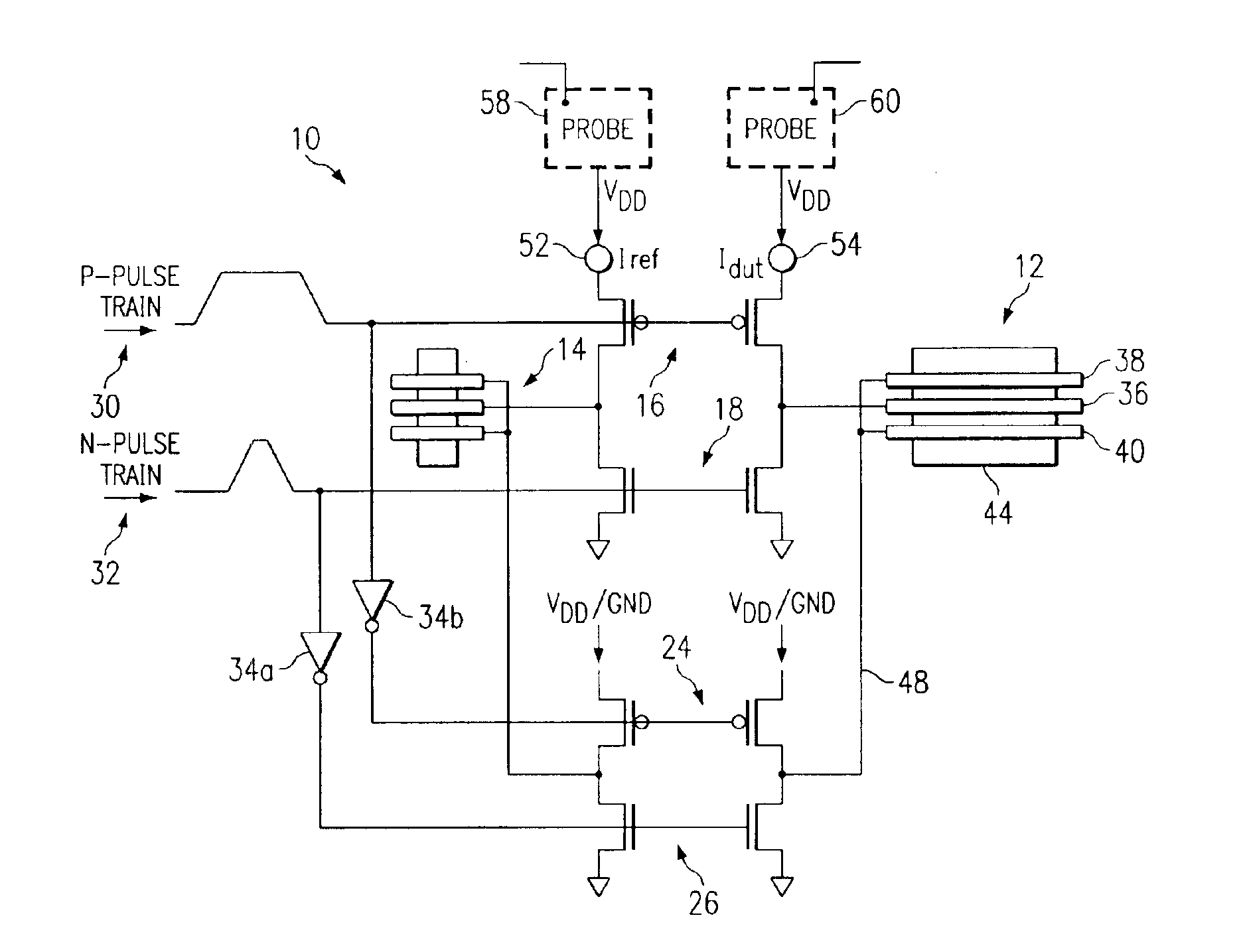
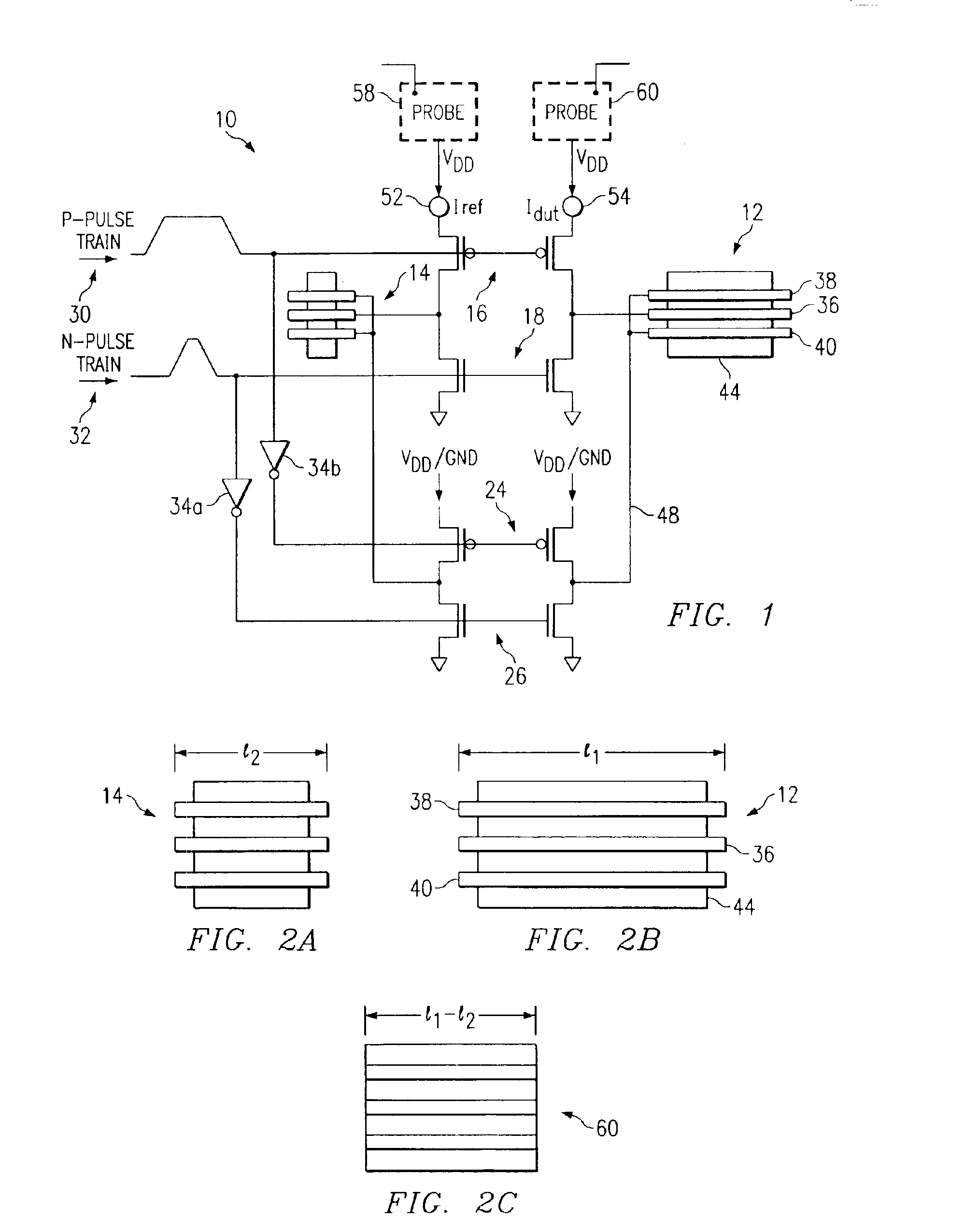
FIG. 1 is a simplified block diagram of a measurement system 10 that may be coupled to an integrated circuit in order to measure a capacitance associated with a portion of the integrated circuit in accordance with one embodiment of the present invention. Measurement system 10 includes a test device 12, a reference structure 14, a first set of p and n element-pairs 16 and 18, and a second set of p and n element-pairs indicated generally at 24 and 26. In general, each element or section within test device 12 may be coupled to an additional set of p and n element-pairs similar to those illustrated in FIG. 1. Measurement system 10 additionally includes a p-pulse train input indicated generally at 30 and an n-pulse train input indicated generally at 32. The pulse trains may be arranged such that when one selected p element is ON, the n element is OFF and when the p element is OFF, the n element is ON.

Measurement system 10 operates to measure a capacitance associated with an element or se...


PUM


Abstract

A method for measuring a capacitance associated with a portion of an integrated circuit is provided that includes coupling a measurement circuit to an integrated circuit. One or more transistors within the integrated circuit are initialized such that a steady-state associated with one or more of the transistors is achieved. A capacitance associated with the portion of the integrated circuit is then measured using the measurement circuit. The portion of the integrated circuit is selectively charged and discharged in response to a voltage potential being applied thereto such that a drain current is generated that serves as a basis for the capacitance measurement.

Description

TECHNICAL FIELD OF THE INVENTIONThis invention relates in general to integrated circuits and more particularly to a system and method for measuring a capacitance associated with an integrated circuit.BACKGROUND OF THE INVENTIONThe design and manufacture of integrated circuits has become increasingly important in the field of semiconductors. Achieving the proper metal capacitance of integrated circuits is critical to the functionality, performance, and reliability of integrated circuits. The ability to closely monitor the manufacture of integrated circuits and semiconductors is similarly important. Semiconductor characteristics or parameters that vary significantly from their designated values may cause significant problems in systems or architectures with precise or exact specifications. Elements associated with transistor specifications, and interconnect specifications including metal thickness, trench width, conductor spacing, and dielectric thickness, represent essential criterio...

Claims


Application Information

Patent Timeline
IPC IPC(8): G01R27/26G01R31/28G01R31/30
CPCG01R27/2605G11C2029/5002G01R31/30G01R31/2851
Inventor SARMA, ROBIN C.DENG, XIAOWEIGALLIA, JAMES DAVID
Owner TEXAS INSTR INC
Why Eureka
Try Eureka