
Process for preparing a multi-layer circuit assembly

Inactive Publication Date: 2002-09-12
PPG IND OHIO INC
View PDF0 Cites 13 Cited by
  • Summary
  • Abstract
  • Description
  • Claims
  • Application Information

AI Technical Summary

Benefits of technology

[0011] It is a further object of the present invention to provide high via density, allowing for more electrical interconnects from highly functional chips to level two packages.
[0012] Additional objects of the present invention include superior dielectric performance and fine line resolution to provide for advanced chip attachment techniques.

Problems solved by technology

As a result, failure of the circuit assembly after repeated use is a risk due to failure of adhesive joints between the layers of the assembly.

Method used


Image

  • Process for preparing a multi-layer circuit assembly
  • Process for preparing a multi-layer circuit assembly
  • Process for preparing a multi-layer circuit assembly

Examples


Embodiment Construction

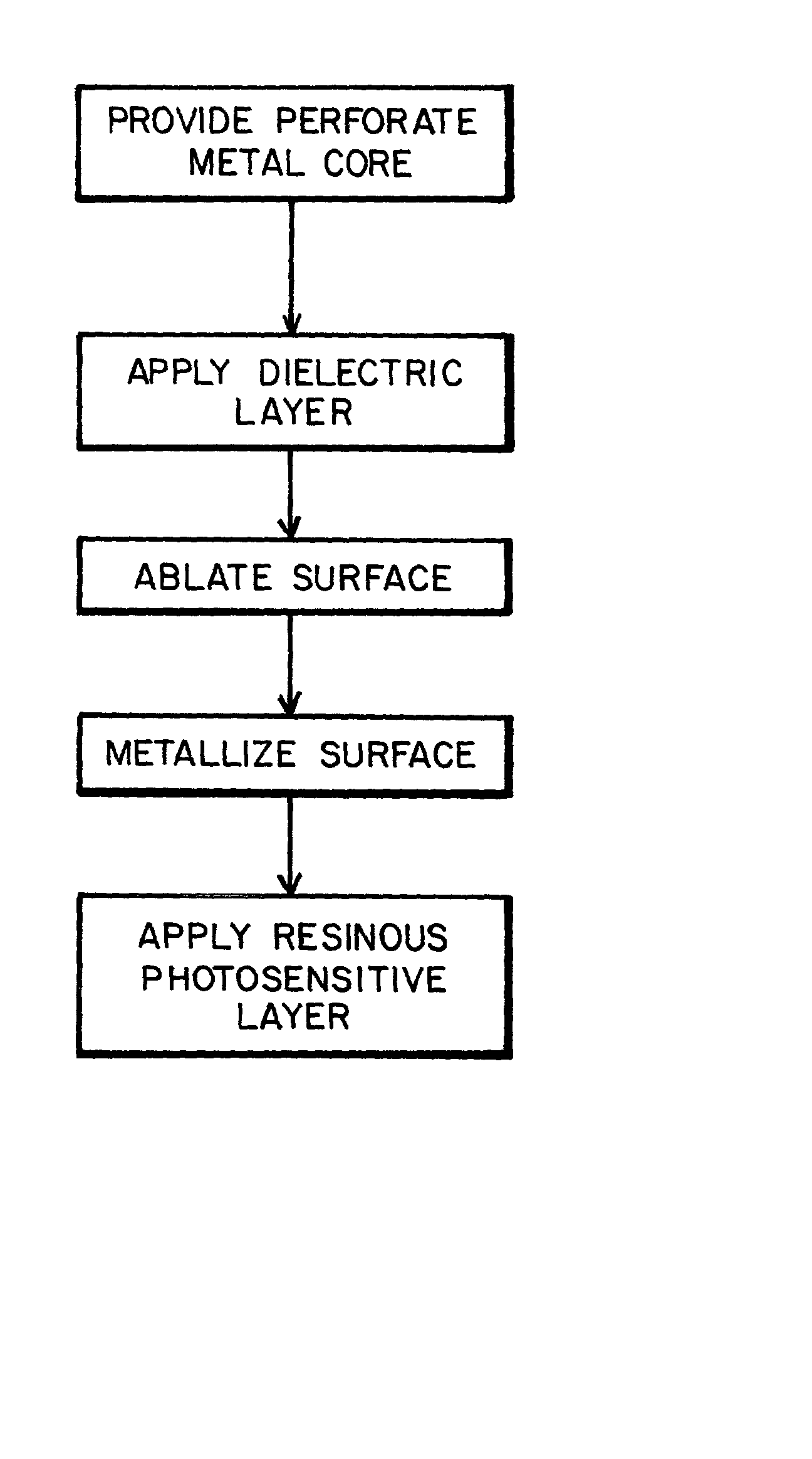
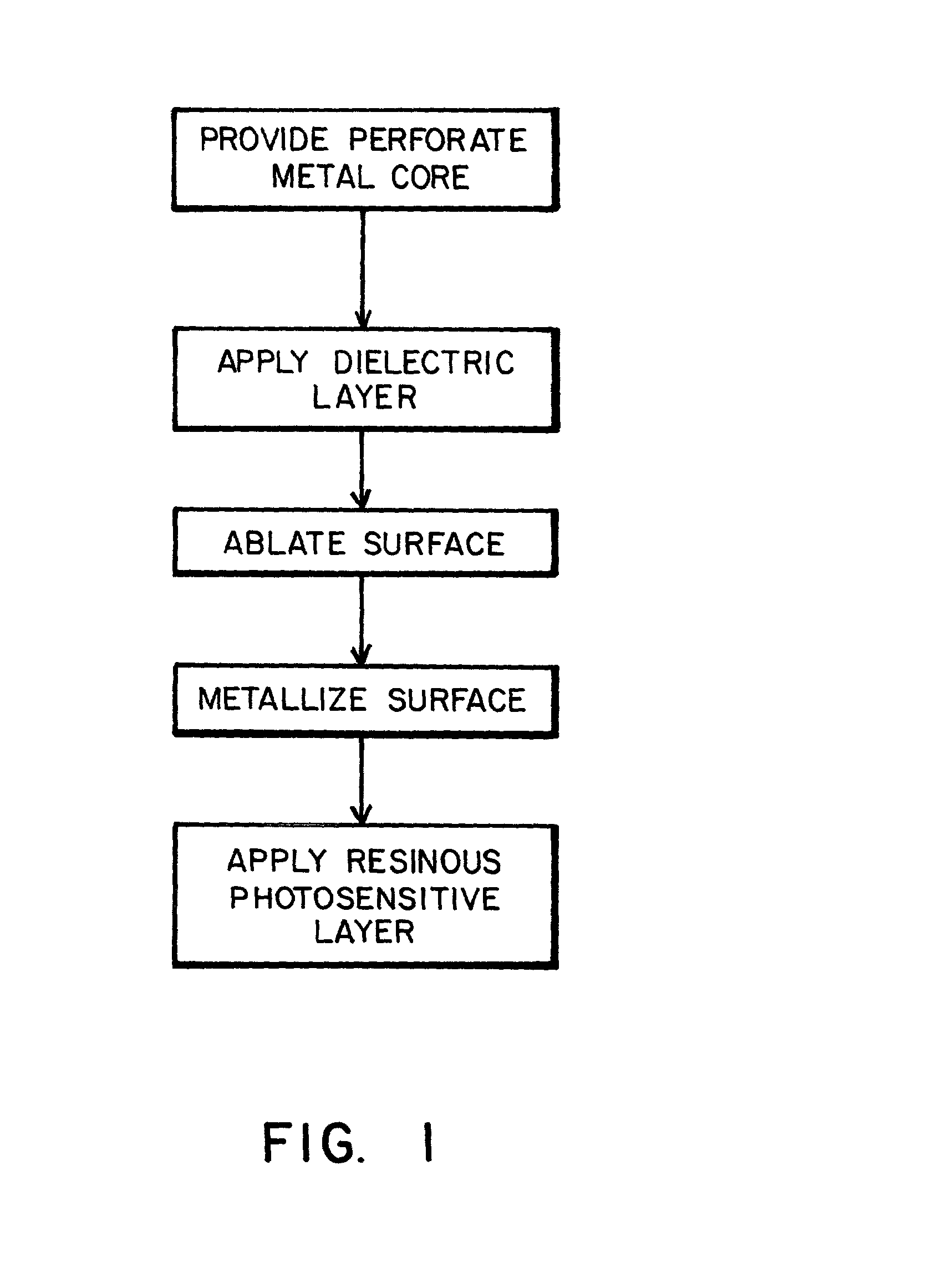
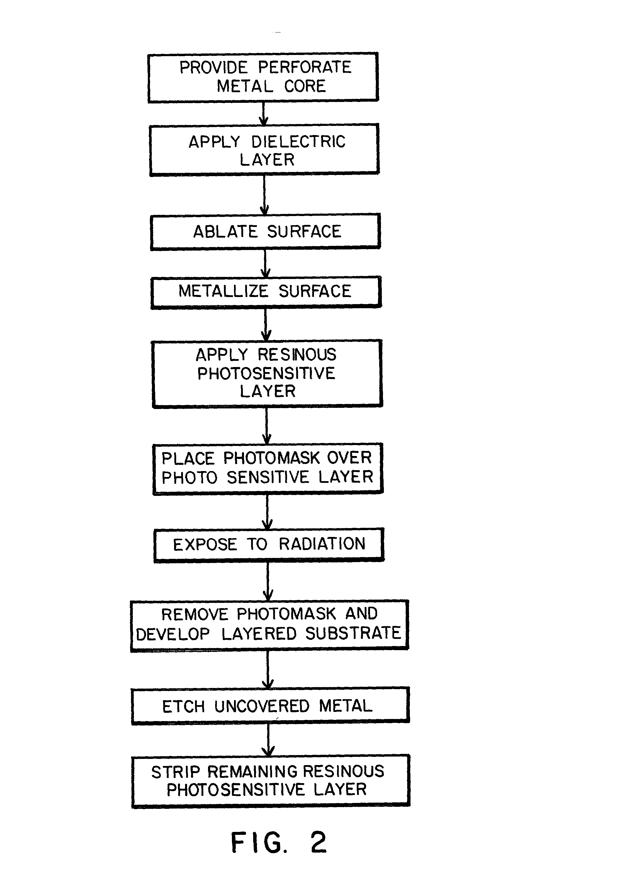
[0021] The process of the present invention for fabricating a multi-layer circuit assembly comprises the following steps:

[0022] (a) providing a perforate metal core;

[0023] (b) applying a dielectric polymer to all exposed surfaces of the metal core to form a conformal coating of substantially uniform thickness on all exposed surfaces of the metal core;

[0024] (c) ablating the surface of the dielectric polymer in a predetermined pattern to expose sections of the metal core;

[0025] (d) applying a layer of metal to all surfaces thereby forming metallized vias through the metal core; and

[0026] (e) applying a resinous photosensitive layer to the metal layer.

[0027] In a separate embodiment, the process of the present invention for fabricating a multi-layer circuit assembly comprises the following steps: (a) through (e) as above;

[0028] (f) placing a photo-mask having a desired pattern over the photosensitive layer to form a layered substrate with selected exposed portions;

[0029] (g) exposing ...


PUM

PropertyMeasurementUnit
Dielectric polarization enthalpyaaaaaaaaaa
Densityaaaaaaaaaa
Adhesion strengthaaaaaaaaaa

Abstract

A process for fabricating a multi-layer circuit assembly is provided comprising the following steps: (a) providing a perforate metal core; (b) applying a dielectric polymer onto all exposed surfaces of the metal core to form a conformal coating of substantially uniform thickness on all exposed surfaces of the metal core; (c) ablating the surface of the dielectric polymer in a predetermined pattern to expose sections of the metal core; (d) applying a layer of metal to all surfaces to form metallized vias through the metal core; and (e) applying a resinous photosensitive layer to the metal layer. Additional processing steps such as circuitization may be included. Circuit assemblies produced by the process of the present invention comprise component layers having high via density and thermal coefficients of expansion that are compatible with those of semiconductor chips and rigid wiring boards which may be attached as components of the circuit assembly.

Description

FIELD OF THE INVENTION[0001] The present invention relates to the field of electronic circuitry, and in particular to preparation of multi-layer circuit assemblies such as chip scale packages.BACKGROUND OF THE INVENTION[0002] An electronic circuit package, or assembly, comprises many individual components including, for example, resistors, transistors, capacitors, etc. These components are interconnected to form circuits, and circuits are likewise interconnected to form units having specific functions. In microelectronic circuit packages, circuits and units are prepared in packaging levels of increasing scale. The smallest scale packaging levels are typically semiconductor chips housing multiple microcircuits and / or other components. Such chips are usually made from ceramics, silicon, and the like. Intermediate package levels ("chip carriers") comprising multi-layer substrates may have attached thereto a plurality of small-scale chips housing many microelectronic circuits. In turn, ...

Claims


Application Information

Patent Timeline
IPC IPC(8): C09D5/44H01L21/48H01L23/14H05K1/05H05K3/00H05K3/38H05K3/42H05K3/44H05K3/46
CPCC09D5/4488H01L21/481H01L21/4857H01L21/486H01L23/142H01L2924/3011H05K1/056H05K3/0023H05K3/0032H05K3/0035H05K3/388H05K3/426H05K3/44H05K3/445H05K3/4608H05K2201/0179H05K2201/09554H05K2201/09609H05K2203/0582H05K2203/135H01L2924/0002H01L2924/00
Inventor STURNI, LANCE C.OLSON, KEVIN C.
Owner PPG IND OHIO INC
Learn More