
Method and apparatus for micro electro-mechanical systems and their manufacture

Inactive Publication Date: 2002-09-12
CORNELL RES FOUNDATION INC
View PDF6 Cites 77 Cited by
  • Summary
  • Abstract
  • Description
  • Claims
  • Application Information

AI Technical Summary

Benefits of technology

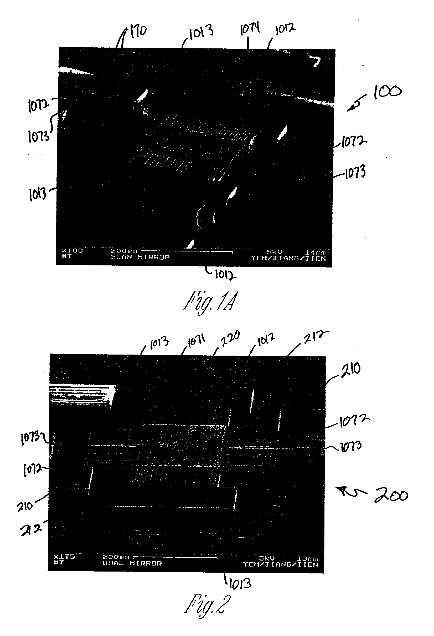
[0010] The present invention provides a fabrication process that integrates high-aspect-ratio silicon structures with polysilicon surface micromachined structures. The process retains not only the high-aspect-ratio silicon structures possible with deep reactive ion etching (DRIE) but also the design flexibility of polysilicon surface micromachining. Using this process, polysilicon platforms have been fabricated, which are actuated by high-aspect-ratio combdrives for many applications such as x-y-z stages and scanning devices. The actuators include an asymmetric combdrive that actuates in torsional / out-of-plane motions, and a high-aspect-ratio combdrive that drives in translational motion.
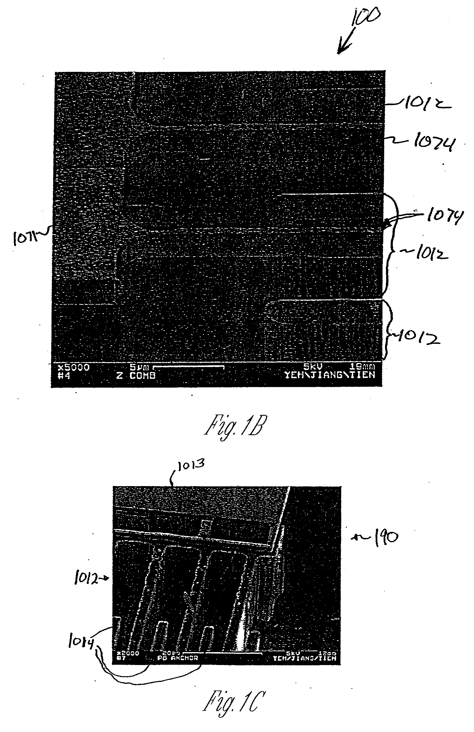
[0014] Another aspect of the present invention provides a fabrication process that integrates polysilicon surface micromachining and DRIE bulk silicon micromachining. It takes advantage of the design flexibility of polysilicon surface micromachining and the deep silicon structures possible with deep reactive ion etching (DRIE). A torsional actuator driven by a combdrive moving in the out-of-plane direction, including polysilicon fingers and bulk silicon fingers, has been fabricated. The integrated process allows the combdrive to be integrated with any structure made by polysilicon surface micromachining. It is found that the driving voltage needed for the combdrive to torsionally actuate a 200 .mu.m by 200 .mu.m membrane is less than that needed for a parallel-plate actuator by at least 30 percent.

Problems solved by technology

However, each of these techniques has its limitations.

Method used


Image

  • Method and apparatus for micro electro-mechanical systems and their manufacture
  • Method and apparatus for micro electro-mechanical systems and their manufacture
  • Method and apparatus for micro electro-mechanical systems and their manufacture

Examples


Embodiment Construction

[0036] In the following detailed description of the preferred embodiments, reference is made to the accompanying drawings that form a part hereof, and in which are shown by way of illustration specific embodiments in which the invention may be practiced. It is understood that other embodiments may be utilized and structural changes may be made without departing from the scope of the present invention.

[0037] The leading digit(s) of reference numbers appearing in the Figures generally corresponds to the Figure number in which that component is first introduced or primarily discussed, such that the same reference number is used throughout to refer to an identical component which appears in multiple Figures. Signals and connections may be referred to by the same reference number or label, and the actual meaning will be clear from its use in the context of the description.

[0038] Definitions:

[0039] Integrated silicon micromachining (forming and shaping very small structures, optionally fo...


PUM


Abstract

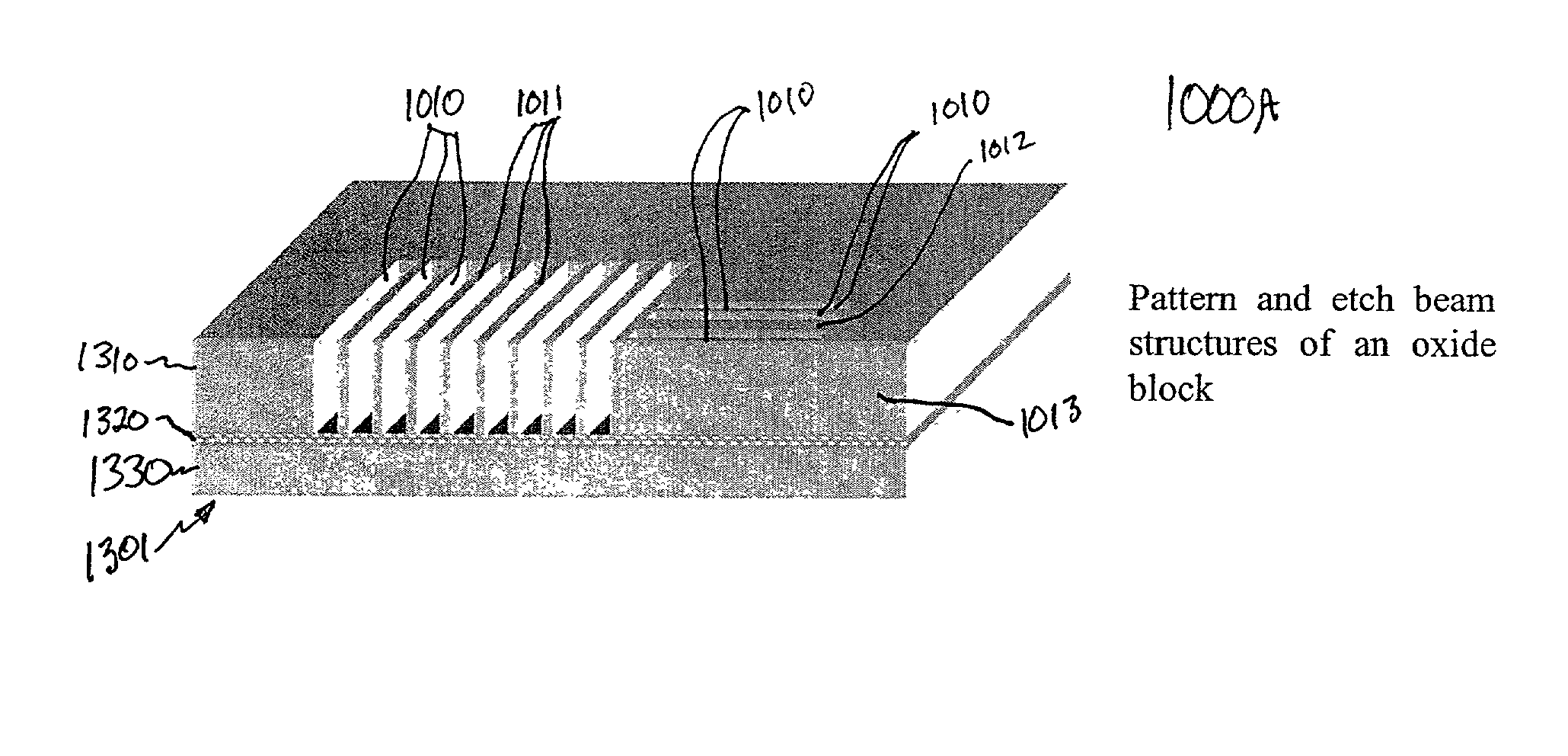
The present invention provides a fabrication process that integrates high-aspect-ratio silicon structures with polysilicon surface micromachined structures. In some embodiments the process includes forming an oxide block by etching a plurality of trenches to leave a plurality of vertical-walled silicon structures standing on the substrate, thermally and substantially completely oxidizing the vertical-walled silicon structures, and substantially filling spaces between the oxidized vertical-walled silicon structures with an oxide of silicon to form the oxide block. The process retains not only the high-aspect-ratio silicon structures possible with deep reactive ion etching (DRIE) but also the design flexibility of polysilicon surface micromachining. Using this process, polysilicon platforms have been fabricated, which are actuated by high-aspect-ratio combdrives for many applications such as x-y-z stages and scanning devices. The actuators include an asymmetric combdrive that actuates in torsional / out-of-plane motions, and a high-aspect-ratio combdrive that drives in translational motion.

Description

CROSS-REFERENCES TO RELATED INVENTIONS[0001] The following commonly assigned U.S. patent applications are relied upon and hereby incorporated by reference in this application:[0002] U.S. Provisional Patent Application No. 60 / 222,511, entitled "METHOD AND APPARATUS FOR MICRO ELECTRO-MECHANICAL SYSTEMS AND THEIR MANUFACTURE" filed Aug. 2, 2000, bearing attorney docket no. 1153.013prv, and[0003] U.S. Patent Application No. ______, entitled "MICROMACHINE DIRECTIONAL MICROPHONE AND ASSOCIATED METHOD" filed on even date herewith, bearing attorney docket no. 1153.030us1.FIELD OF THE INVENTION[0004] This invention relates to the field of micromechanical sensors, and more specifically to a method and apparatus for making micromechanical devices using a sacrificial oxide block.Background of the Invention[0005] Microelectromechanical systems (MEMS) refers to a technology in which electrical and mechanical devices are fabricated at substantially microscopic dimensions utilizing techniques well ...

Claims


Application Information

Patent Timeline
IPC IPC(8): B81B3/00H04R19/00
CPCB81B2203/0136B81C1/00182B81C1/00619B81C2201/0132B81C2201/0178B81C2201/056H04R19/005
Inventor YEH, JER-LIANGTIEN, NORMAN C.
Owner CORNELL RES FOUNDATION INC
Learn More