Method to form bump in bumping technology

a technology of bumping and soldering, which is applied in the direction of semiconductor devices, semiconductor/solid-state device details, electrical apparatus, etc., can solve the problems of difficult to obtain small diameter openings in the (relatively) thick layer of dry photoresist, difficult to apply dry resist layers, and difficult to adhere to the surface of semiconductor substrates

Inactive Publication Date: 2002-09-12
TAIWAN SEMICON MFG CO LTD
View PDF7 Cites 39 Cited by
  • Summary
  • Abstract
  • Description
  • Claims
  • Application Information

AI Technical Summary

Benefits of technology

[0023] A principle objective of the invention is to provide a cost reduced method of creating interconnect bumps.
[0024] Another objective of the invention is to provide a process for creating interconnect bumps that allows for the creation of very fine pitch interconnect bumps.
[0025] Yet another objective of the invention is to provide a process for creating interconnect bumps that eliminates the expense that is incurred using processes of electroplating for the creation of interconnect bumps.
[0026] A still further objective of the invention is to provide a process for creating interconnect bumps that eliminates the disadvantage that is incurred when using screen printing techniques of not being able to create very fine pitch interconnect bumps.
[0028] In accordance with the objectives of the invention, a new method and processing sequence is provided for the creation of interconnect bumps. A layer of passivation is deposited over a contact pad and patterned, creating an opening in the layer of passivation that aligns with the contact pad. A layer of UBM metal is deposited over the layer of passivation, the layer of UBM is overlying the contact pad and limited to the immediate surroundings of the contact pad. The central surface of the layer of UBM is selectively electroplated after which a layer of solder or solder alloy is solder printed over the electroplated surface of the layer of UBM. A solder flux or paste is applied over the surface of the solder printed solder compound or solder alloy. Flowing of the solder or solder alloy creates the solder bump of the invention.

Problems solved by technology

For the dry resist method, the minimum thickness of the layer of dry photoresist is in the range of 75 to 100 microns, making it difficult to obtain openings of small diameter in the (relatively) thick layer of dry photoresist.
Where however smaller geometries are used, such as on the surface of a semiconductor device, the dry resist method does not provide for an interconnect bump with a small enough diameter.
In addition, dry resist layers are difficult to apply and adhere to the surface of semiconductor substrates.
This too however runs into problems where small geometries are required for the to be created elevated point of electrical contact.
The metal mask presents problems of size limitations because the openings that can be created in the surface of the metal mask cannot be created small enough such that small enough diameter interconnect bumps can be created.
In addition, masking techniques invariably present problems of alignment, these problems are further aggravated where very small geometries are required or where a dense pattern of interconnect bumps is to be created.

Method used


Image

  • Method to form bump in bumping technology
  • Method to form bump in bumping technology
  • Method to form bump in bumping technology

Examples


Embodiment Construction

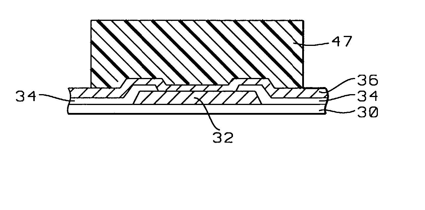
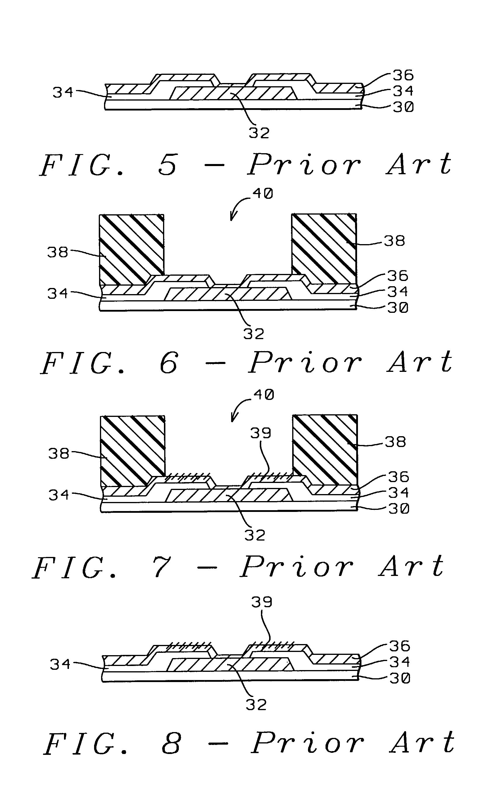
[0049] Referring now specifically to FIG. 5, there is shown a cross section of a semiconductor surface 30 on which:

[0050] a contact pad 32 has been provided

[0051] a layer 34 of passivation has been deposited over the semiconductor surface 30 and has been patterned and etched partially exposing the surface of the aluminum pad 32

[0052] in-situ sputter clean has been performed of the exposed surface of the contact pad (not shown in FIG. 5)

[0053] a seed layer (not shown in FIG. 5) has been blanket deposited over the surface of the layer 34 of passivation including the exposed surface of the contact pad 32, and

[0054] a film 36 of Under Ball Metallurgy has been blanket deposited over the seed layer.

[0055] Layer 30 is the surface of a semiconductor layer, a contact pad 32 has been created on surface 30. Surface 30 will typically be the surface of a semiconductor substrate, the surface of an interconnect substrate and the like. A contact pad 32 has been created on surface 30, electrical con...


PUM

PropertyMeasurementUnit
thicknessaaaaaaaaaa
thicknessaaaaaaaaaa
pressureaaaaaaaaaa

Abstract

A new method and processing sequence is provided for the creation of interconnect bumps. A layer of passivation is deposited over a contact pad and patterned, creating an opening in the layer of passivation that aligns with the contact pad. A layer of UBM metal is deposited over the layer of passivation, the layer of UBM is overlying the contact pad and limited to the immediate surroundings of the contact pad. The central surface of the layer of UBM is selectively electroplated after which a layer of solder or solder alloy is solder printed over the electroplated surface of the layer of UBM. A solder flux or paste is applied over the surface of the solder printed solder compound or solder alloy. Flowing of the solder or solder alloy creates the solder bump of the invention.

Description

BACKGROUND OF THE INVENTION[0001] (1) Field of the Invention[0002] The invention relates to the fabrication of integrated circuit devices, and more particularly, to a method of forming solder bumps whereby plating is used to create Under Ball Metallurgy and printing is used for creating the solder ball.[0003] (2) Description of the Prior Art[0004] The present invention addresses a method of forming an electrical interconnection and, more particularly, a method of forming an interconnect bump. The method of the present invention can be used for the creation of electrical contacts on the surface of semiconductor devices but is not limited to such applications. The method of the present invention can equally be applied to form raised electrical contacts on semiconductor substrates, printed circuit boards, flex circuits or a metallized or glass substrate or semiconductor device mounting support. In its present form the method of the invention is most favorably applied to the creation of...

Claims


Application Information

Patent Timeline
Patent Type & Authority Applications(United States)
IPC IPC(8): H01L21/60
CPCH01L24/11H01L24/12H01L2224/1147H01L2224/11902H01L2224/13023H01L2224/13099H01L2924/01013H01L2924/01015H01L2924/01018H01L2924/01022H01L2924/01029H01L2924/01078H01L2924/01079H01L2924/01082H01L2924/04941H01L2924/14H01L2924/3025H01L2224/05027H01L2224/05022H01L2924/01005H01L2924/01006H01L2924/01019H01L2924/01024H01L2924/01033H01L2924/014H01L2224/05568H01L2924/0002H01L2224/05552H01L2224/131H01L2224/0401
Inventor LIN, KUO-WEICHU, CHENG-YUCHEN, YEN-MINGFAN, YANG-TUNGFAN, FU-JIERPENG, CHIOU SHIANLIN, SHIH-JANG
Owner TAIWAN SEMICON MFG CO LTD
Why Eureka
Try Eureka