Plasma display panel with an improved electrode structure

a technology of electrode structure and display panel, which is applied in the direction of electrodes, tubes with screens, gas-filled discharge tubes, etc., can solve the problems of insufficient wall charge quantity, inability to sustain discharge, and insufficient quantity of wall charge, so as to improve cell structure, improve display quality, and improve cell structure

Inactive Publication Date: 2002-09-19
PIONEER CORP
View PDF3 Cites 12 Cited by
  • Summary
  • Abstract
  • Description
  • Claims
  • Application Information

AI Technical Summary

Benefits of technology

[0048] It is a further object of the present invention to provide a novel plasma display panel improved in display quality.
[0050] It is yet a further object of the present invention to provide a novel plasma display panel having an improved cell structure for obtaining an improved display quality.

Problems solved by technology

The gradual decease of the effective voltage level results in no longer possible of sustaining the discharge, whereby the discharge will be discontinued in the course of time.
The reduction in the quantity of the wall charges has to be made so that the reduced quantity of the wall charges does not prevent the subsequent write discharge and the sustaining discharge.
Notwithstanding, this write discharge is a weak discharge having a low degree of ionization, thereby forming an insufficient quantity of the wall charges for prompt transition from the write discharge to the sustaining discharge.
If the write voltage or the potential difference between the data electrodes and the scanning electrodes is increased to cause the strong discharge having a high degree of ionization, then an insufficient quantity of the wall charges is formed for prompt transition from the write discharge to the sustaining discharge.
Once the large quantity of the wall charges is formed over the entirety of the surface electrode, the wall charges on the surface electrodes provide an undesirable influence to adjacent cells, thereby causing a discharge interference.
This discharge interference may cause erroneous light-on and light-off.
The unnecessary charge and discharge are increased in connection with the write discharge, resulting in an increased power consumption.
If the sustaining voltage level or a potential difference between the sustaining electrodes and the scanning electrodes is increased in place of increasing the write voltage, then undesirable discharges are likely to be caused in non-selected cells.
The unnecessary charge and discharge are increased in connection with the write discharge, resulting in an increased power consumption.
The spread of the sustaining discharge is excessively wide, thereby causing a discharge interference.
This discharge interference may cause erroneous light-on and light-off.
If the electrode area in the vicinity of the surface discharge gap is excessively small, then the insufficient quantity of the wall charges is formed, resulting in undesirable increase of the sustaining voltage and narrowing the available voltage range for performing the required memory function.
This conventional structure makes it difficult that the electrodes exhibit optimum respective performances in the different rolls.

Method used


Image

  • Plasma display panel with an improved electrode structure
  • Plasma display panel with an improved electrode structure
  • Plasma display panel with an improved electrode structure

Examples


first embodiment

[0107]

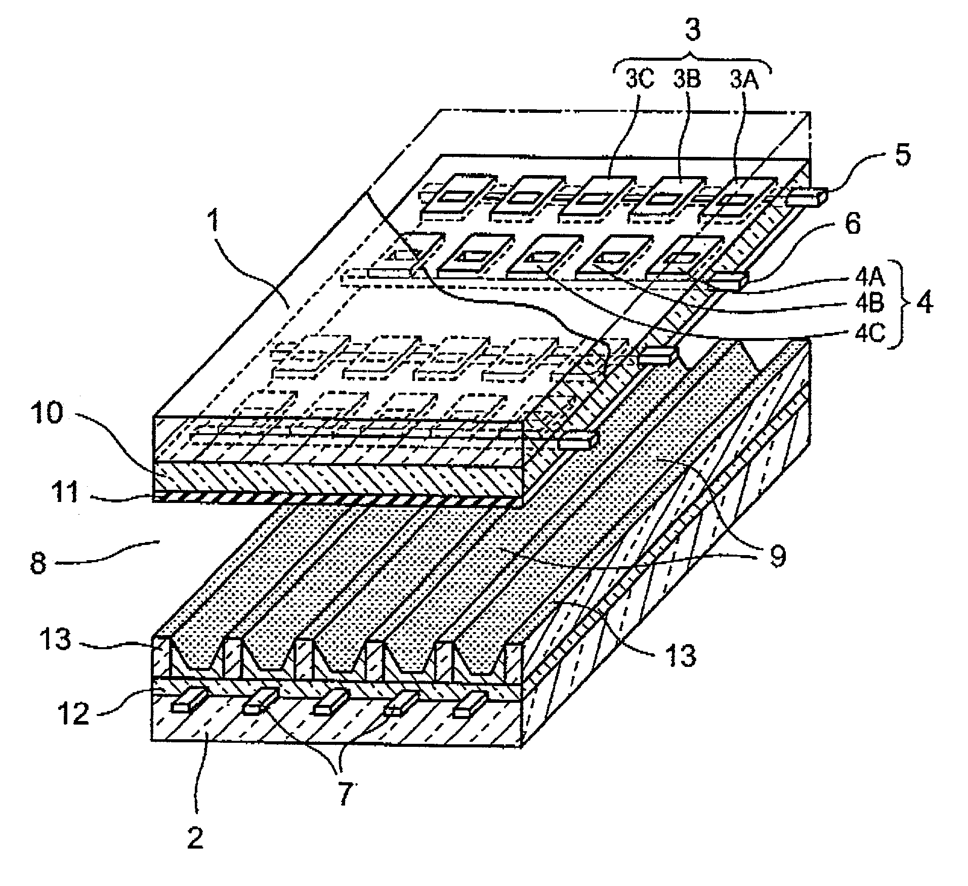
[0108] A first embodiment according to the present invention will be described in detail with reference to the drawings. FIG. 9 is a perspective view illustrative of a panel structure of a novel plasma display panel in accordance with the present invention.

[0109] The novel plasma display panel has a front side insulative substrate 1 and a back side insulative substrate 2. A plurality of scanning electrode alignments 3 and a plurality of sustaining electrode alignments 4 are provided on an inside face of the front side insulative substrate 1. The scanning electrode alignments 3 and the sustaining electrode alignments 4 are alternately placed at a predetermined pitch in a first horizontal direction. The scanning electrode alignments 3 and the sustaining electrode alignments 4 extend in parallel to each other and in a second horizontal direction which is perpendicular to the first horizontal direction.

[0110] Each of the scanning electrode alignments 3 further comprises scanning e...


PUM


Abstract

A plasma display panel has an improved cell electrode structure including: a pair of sustaining and scanning electrodes which are approximately similar or equal in area to each other, and which are different from each other in pattern shape. Each of the scanning electrode alignments further includes a plurality of scanning electrodes. Adjacent two of the scanning electrodes are separated from each other by the separation wall. Each of the sustaining electrode alignments further includes a plurality of sustaining electrodes. Adjacent two of the sustaining electrodes are separated from each other by the separation wall.

Description

BACKGROUND OF THE INVENTION[0001] 1. Field of the Invention[0002] The present invention relates to a plasma display panel, and more particularly to an alternating current surface discharge plasma display panel having an asymmetrical plane electrode structure.[0003] 2. Description of the Related Art[0004] The plasma display panel has been known as a thin flat screen display device having a large screen size and a large capacity. Electrons are accelerated by an electric field so that the accelerated electrons have collisions to a discharge gas to cause excitation and subsequent relaxation. This relaxation process causes radiation of an ultraviolet ray. The ultraviolet ray is irradiated onto a fluorescent material, whereby the ultraviolet ray is converted into a visible light. The alternating current plasma display panel is generally superior in luminance, luminous efficiency and operational life-time than the direct current plasma display panel.[0005] FIG. 1 is a perspective view illu...

Claims


Application Information

Patent Timeline
Patent Type & Authority Applications(United States)
IPC IPC(8): H01J11/12H01J11/14H01J11/22H01J11/24H01J11/26H01J11/34
CPCH01J11/12H01J11/24H01J2211/245H01J2211/323
Inventor HASEGAWA, HIROSHIAIBARA, NOBUMITSUHIRANO, NAOTONAKAMURA, TADASHITANAKA, YOSHITOHOMMA, HAJIMEARAKI, KOTA
Owner PIONEER CORP
Why Eureka
Try Eureka