Semiconductor integrated circuit manufacturing method and model parameter extracting method, apparatus, and program
a technology of integrated circuits and model parameters, applied in the field of semiconductor integrated circuit manufacturing methods and model parameter extraction methods, apparatuses, programs, etc., can solve the problems of difficult to realize a perfectly localized state, involving local solutions of poor accuracy when handling many parameters, and requiring a lot of time and money to test these circuits
- Summary
- Abstract
- Description
- Claims
- Application Information
AI Technical Summary
Problems solved by technology
Method used
Image


Examples
example)
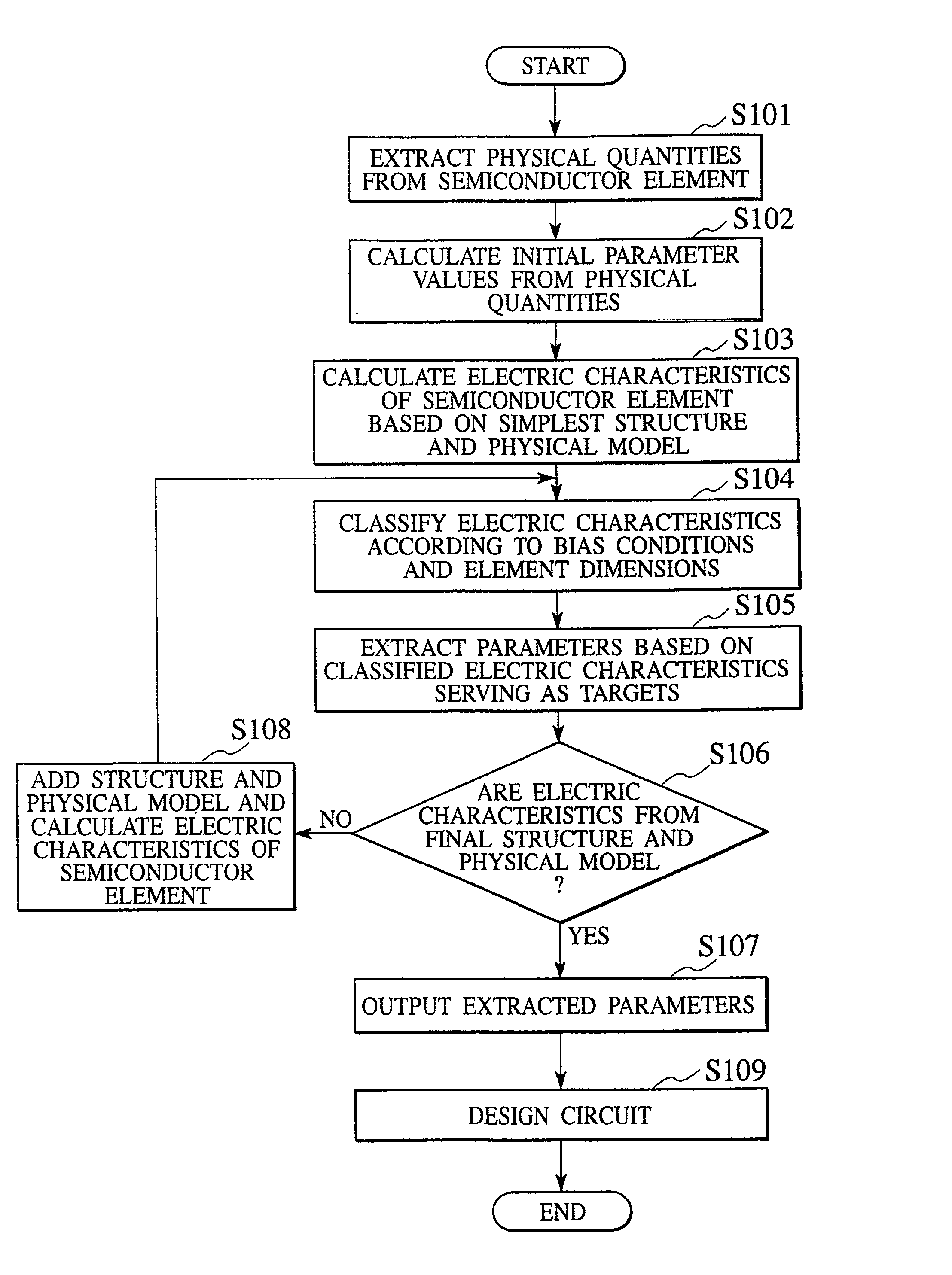
[0052] (Example)
[0053] The parameter extracting technique of the present invention will be explained in more detail with reference to an experimental example. The example extracts parameters of a BSIM3v3 model representing a MOSFET. An example of configuration of the MOSFET is shown in FIG. 5.
[0054] The MOSFET encompassing, for example a p type substrate 71, and an n.sup.+ source region 72 and an n.sup.+ drain region 73 disposed at a surface of and in the p type substrate 71. A metallic source electrode 76 and a metallic drain electrode 78 are contacted to the surface of the n+ source region 72 and the n.sup.+ drain region 73, respectively. An gate oxide film 75 is formed on the surface of the p substrate 71 between the n.sup.+ source region 72 and the n+ drain region 73, and the gate electrode 77 is disposed on the gate oxide film 75. A channel region 74 is defined between the n.sup.+ source region 72 and the n.sup.+ drain region 73 serving as a path of the main current which flows...
PUM
 Abstract
Description
Claims
Application Information