Thin-film thermoelectric cooling and heating devices for DNA genomic and proteomic chips, thermo-optical switching circuits, and IR tags

a technology of thermoelectric cooling and heating devices, which is applied in the direction of thermoelectric device details, surgical instruments for heating, apparatus with spatial temperature gradients, etc., can solve the problems of not being able to selectively heat or cool local regions without thermoelectric devices, and not being able to employ thermoelectric devices in applications requiring selective heating or cooling, etc., to achieve rapid heating or cooling

Active Publication Date: 2002-11-28
LAIRD THERMAL SYST INC
View PDF39 Cites 70 Cited by
  • Summary
  • Abstract
  • Description
  • Claims
  • Application Information

AI Technical Summary

Benefits of technology

0009] Still another object of the present invention is to provide rapid heating or cooling to selective surface components.
0010] Another object of the pres...

Problems solved by technology

So far, bulk thermoelectric devices have not been made to selectively heat or cool local regions without heating or cooling adjacent areas because of their relatively large si...

Method used


Image

  • Thin-film thermoelectric cooling and heating devices for DNA genomic and proteomic chips, thermo-optical switching circuits, and IR tags
  • Thin-film thermoelectric cooling and heating devices for DNA genomic and proteomic chips, thermo-optical switching circuits, and IR tags
  • Thin-film thermoelectric cooling and heating devices for DNA genomic and proteomic chips, thermo-optical switching circuits, and IR tags

Examples


Embodiment Construction

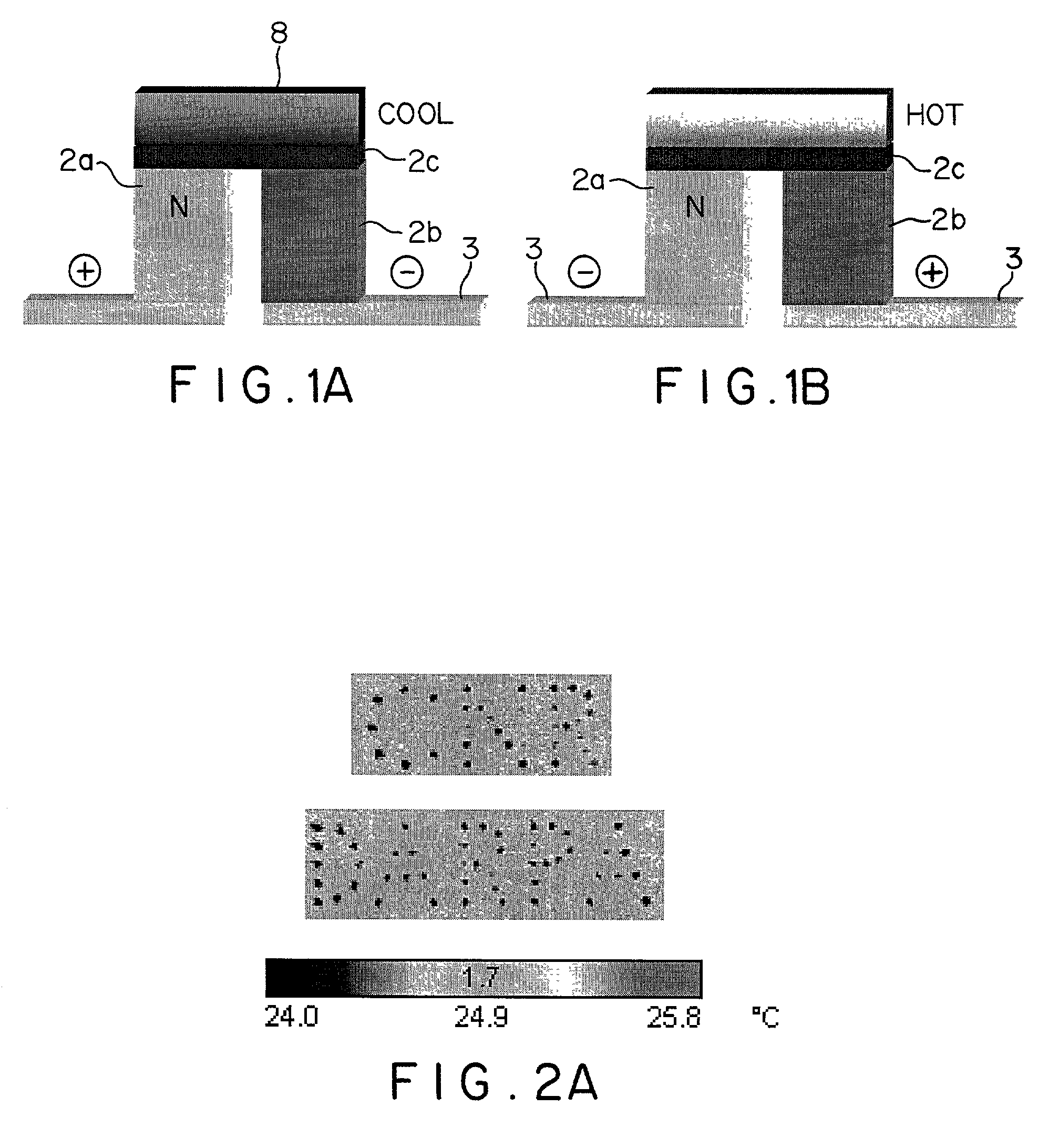
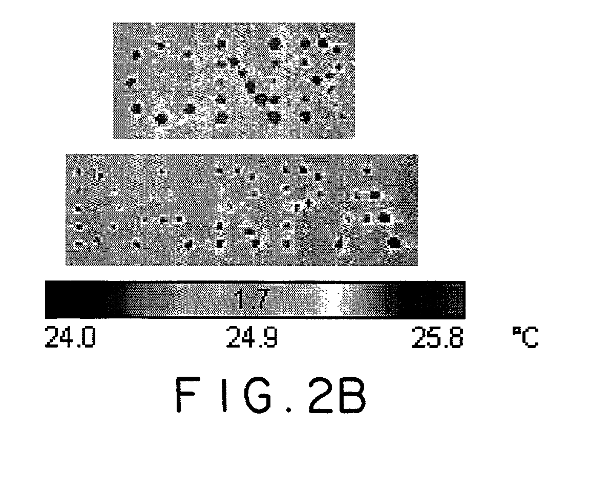
[0036] Referring now to the drawings, wherein like reference numerals designate identical, or corresponding parts throughout the several views, and more particularly to FIG. 2A thereof, FIG. 2A is an illustration of a spot cooled image in the form of "ONR" and "DARPA" as shown by an IR image feature produced by cooling of the present thermoelectric devices. In such cooling, microelectronic lithography is employed to pattern micro thermoelements arbitrarily across the surface of a substrate. The second illustration in FIG. 2B shows an infra-red image generated by spot heating in a thermoelectronic device of the present invention. The ability to obtain spot cooling or heating with thin-film thermoelements is enabled by the very low-resistivity specific contact resistivities leading to relatively high device (which includes the effect of contact resistance and that of the material) figure-of-merit (ZT>0.1 at 300K) which can be obtained with the thin-film thermoelements. By reversal of ...


PUM

PropertyMeasurementUnit
Lengthaaaaaaaaaa
Lengthaaaaaaaaaa
Timeaaaaaaaaaa

Abstract

A thermoelectric cooling and heating device including a substrate, a plurality of thermoelectric elements arranged on one side of the substrate and configured to perform at least one of selective heating and cooling such that each thermoelectric element includes a thermoelectric material, a Peltier contact contacting the thermoelectric material and forming under electrical current flow at least one of a heated junction and a cooled junction, and electrodes configured to provide current through the thermoelectric material and the Peltier contact. As such, the thermoelectric cooling and heating device selectively biases the thermoelectric elements to provide on one side of the thermolectric device a grid of localized heated or cooled junctions.

Description

[0001] This application claims priority under 35 U.S.C. .sctn.119 to U.S. Provisional Application No. 60 / 282,185 entitled Thin-film Thermoelectric Cooling and Heating Devices for DNA Genomic and Protemic Chips, Thermo-optical Switching Circuits, and IR Tags, filed Apr. 9, 2001, the entire contents of which are incorporated herein by reference. This application includes subject matter related to that disclosed in U.S. Pat. No. 6,071,351; and U.S. Ser. No. 09 / 381,963, filed Mar. 31, 1997, entitled Thin-film Thermoelectric Device and Fabrication Method of Same; and U.S. Provisional Application Serial No. 60 / 190,924, filed March 2000, entitled Cascade Thermoelectric Cooler; and U.S. Serial No. 60 / 253,743, filed Nov. 29, 2000, entitled Spontaneous Emission Enhanced Heat Transport Method and Structure for Cooling, Sensing, and Power Generation, the entire contents of which are incorporated herein by reference.[0002] 1. Field of the Invention[0003] The present invention relates to thin-fil...

Claims


Application Information

Patent Timeline
IPC IPC(8): B01L3/00B01L7/00C12M1/00C12M1/34G02F1/01C12M1/38C12N15/09F25B21/04H01L23/38H01L27/146H01L35/08H01L35/30H01L35/32H01S5/024H01S5/065H01S5/183H01S5/187H05B3/10
CPCB01L3/5085B01L7/52H01L2924/1461B01L7/54B01L2400/0448F25B21/04H01L23/38H01L27/14649H01L35/08H01L2224/95147H01L2924/01077H05B3/10H01L2924/01019H01L2924/01068H01L2224/95145H01L2924/00H10N10/817C12Q1/68B82B3/00
Inventor VENKATASUBRAMANIAN, RAMA
Owner LAIRD THERMAL SYST INC
Why Eureka
Try Eureka