Noise suppression circuit, asic, navigation apparatus, communication circuit, and communication apparatus having the same

a technology of noise suppression circuit and communication circuit, which is applied in the direction of code conversion, pulse technique, instruments, etc., can solve the problems of noise generation, counter-plan of urgent necessity, and the largest possibility of conductor noise from the power supply line to have a bad influence on other electronic devices

Inactive Publication Date: 2003-01-16
KK TOSHIBA
View PDF21 Cites 13 Cited by
  • Summary
  • Abstract
  • Description
  • Claims
  • Application Information

AI Technical Summary

Problems solved by technology

The generation of an EMI (electromagnetic interference) noise may cause another electronic apparatus to be erroneously operated, which may result in a serious trouble.
Among them, the conduction noise from the power supply line has the largest possibility of having a bad influence on other electronic apparatuses.
Thus, the counter-plan thereof is of urgent necessity.
As for this conduction noise from the power supply line, a change of a signal inputted to a circuit causes the power supply current to be changed, which results in the generation of the noise.
However, especially, since many latches used in an integrated circuit are simultaneously operated in synchronization with a clock, the power supply current suddenly flows to thereby generate the switching noise.
At this time, if the capacitance of the bypass capacitor C is small and a load current is large, the switching noise may exceed an allowable value.
However, it is conventionally difficult to insert the bypass capacitor having the large capacitance in the view of a limitation of a chip area, a cost and the like when the RC filter is inserted into the chip of the LSI.
After all, the consideration of the chip area and the cost leads to the unavoidable utilization of the bypass capacitor having the small capacitance for them.
In this case, it is very difficult to sufficiently suppress the switching noise generated by the sudden change of the power supply current.
Accordingly, other electronic apparatuses may be erroneously operated by the EMI noise generated in the semicustom LSI.
However, the capacitance of the bypass capacitor per unit area on a device formation surface can not be made so large.
For this reason, the capacitance necessary for the noise filter can not be obtained, and further the switching noise can not be sufficiently suppressed.
That is, this implies that it is impossible to attain the sufficient effect for the suppression of the EMI noise.
Hence, it is technically difficult to freely form the bypass capacitor cells on the chip.
Now, there is no method to effectively suppress the EMI noise.
However, there is no attempt of using this type capacitor as the bypass capacitor to suppress the noise.
If the currents having the same direction simultaneously run through many signal lines of the data buses, a strong EMI noise is generated.
As a result, it is difficult to insure the stable operation of the circuit.
This results in the problem of the increase of the number of the data buses.

Method used


Image

  • Noise suppression circuit, asic, navigation apparatus, communication circuit, and communication apparatus having the same
  • Noise suppression circuit, asic, navigation apparatus, communication circuit, and communication apparatus having the same
  • Noise suppression circuit, asic, navigation apparatus, communication circuit, and communication apparatus having the same

Examples


first embodiment

[0134] (First Embodiment)

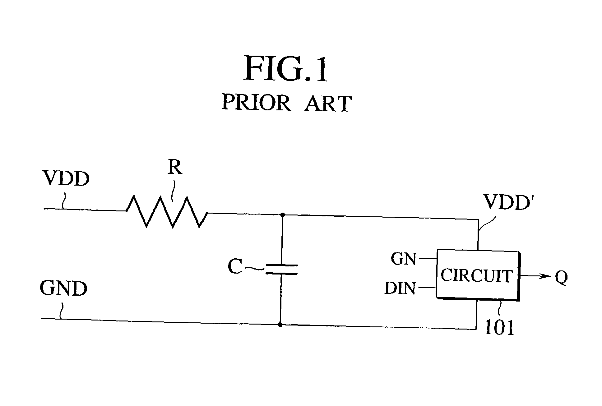
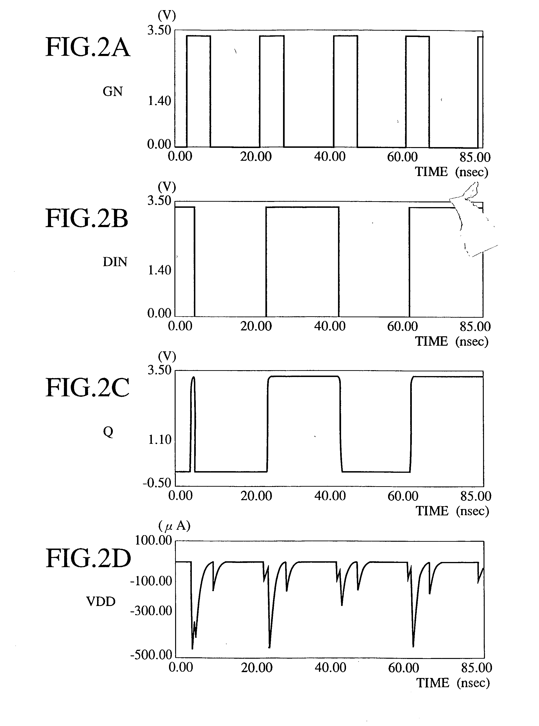
[0135] FIG. 10 is a circuit diagram of a switching noise suppression circuit 790 according to a first embodiment of the present invention. The switching noise suppression circuit (noise filter) 790 in the first embodiment of the present invention comprises an internal circuit 1, a first transistor 12, a second transistor 11 and a bypass capacitor C. The internal circuit has a high level terminal V.sub.DD' and a low level terminal wherein the low level terminal is connected to a low level power supply line GND. The first transistor 12 and second transistor 11 are connected in series between a high level power supply line V.sub.DD and the internal circuit 1. That is, one main electrode of the first transistor 12 is connected to the high level terminal V.sub.DD' of the internal circuit. The bypass capacitor C is connected between the low level power supply line GND and a node N situated midway between the other main electrode of the first transistor 12 and seco...

second embodiment

[0140] (Second Embodiment)

[0141] FIG. 12 is a circuit diagram of a switching noise suppression circuit 790 according to a second embodiment of the present invention. Then, the same or similar reference numerals are applied to the elements common to those in FIG. 1, and the explanations thereof are omitted.

[0142] As for a noise filter according to the second embodiment of the present invention, a limiter resistor R is inserted in series between the second transistor 11 and the node N in the configuration of FIG. 10. In the first embodiment of the present invention, it is necessary to make a length of a gate of the second transistor 11 longer, in order to make the on-state resistance r.sub.DS(on) of the second transistor 11 larger, which results in the increase of the circuit formation area. However, since the limiter resistor R is inserted in the second embodiment of the present invention, the on-state resistance r.sub.DS(on) of the second transistor 11 can be made correspondingly sm...

third embodiment

[0146] (Third Embodiment)

[0147] FIGS. 13A, 13B and 13C are views to explain a switching noise suppression circuit 790 according to a third embodiment of the present invention. That is, FIG. 13A is a circuit diagram of the switching noise suppression circuit, FIG. 13B is a configuration view of a signal generation circuit of an enable signal GN and FIG. 13C is a view showing a waveform of a clock signal CLK.

[0148] As for a noise filter according to the third embodiment of the present invention, the internal circuit 1 is constituted by a latch. And a resistor 21 is connected in parallel to the configuration in FIG. 12 explained in the second embodiment. Namely, the resistor 21 is connected parallel to the second transistor 11, the limiter resistor R and the first transistor 12 between the high level power supply line V.sub.DD and the latch 1.

[0149] This resistor 21 is mounted to supplement a current by considering a leak current I.sub.LEAK generated when the state of the latch 1 is he...


PUM


Abstract

The present invention provides an noise suppression circuit comprises an internal circuit which has a high and a low level terminals. The low level terminal is connected to a low level power supply (GND) line. The noise suppression circuit further comprises a first transistor in which one main electrode is connected to the high level terminal of the circuit, a bypass capacitor connected between the other main electrode of the first transistor and the low level power supply line, and a second transistor connected between the other main electrode of the first transistor and a high level power supply (VDD) line. The first transistor is conductive when the internal circuit is active, and is not conductive when the internal circuit is inactive. The second transistor is not conductive when the internal circuit is active, and is conductive when the internal circuit is inactive. Moreover, a communication circuit for setting the number of data buses to be newly added to be less than two times a transmission data, then encoding the data to be sent so as to make the numbers of "0" and "1" in the data to be sent through the data buses equal to each other and accordingly reducing the increase of the number of the data buses to a minimum and thereby suppressing the common phase power supply noise is provided. A communication apparatus comprising the communication circuit is also provided. Furthermore, the bypass capacitor C for noise suppression circuit is formed in an empty space in a ASIC. A polysilicon layer constituting one electrode of the bypass capacitor is formed in the substrate contact region formed between basic cells regularly arranged, each including a plurality of nMOS and pMOS transistors. This bypass capacitor C is connected between the high and the low level power supply lines to reduce the current running through the power supply line to suppress the EMI noise.

Description

[0001] 1. Field of the Invention[0002] The present invention relates to a technique to suppress an electromagnetic radiation noise, and more particularly to a switching noise suppression circuit to suppress a switching noise of a circuit in which an activation and a inactivation are repeated by an enable signal, a built-in noise filter type data holding circuit in which this switching noise suppression circuit is built, a car navigation apparatus which comprises this built-in noise filter type data holding circuit, a communication circuit for sending and receiving a digital signal through data buses and a communication apparatus which comprises this circuit. Moreover, the present invention relates to a technique to suppress an electromagnetic radiation noise in an application-specific integrated circuit (ASIC).[0003] 2. Description of the Related Art[0004] Recently, an environment problem of an electromagnetic radiation has been largely taken up. The generation of an EMI (electromag...

Claims


Application Information

Patent Timeline
Patent Type & Authority Applications(United States)
IPC IPC(8): H03K17/16H04H60/04
CPCH03K17/162H03K19/00361
Inventor TAKEUCHI, HIDEKIMURAKATA, MASAMIYAMADA, MASAAKINOJIMA, REIKOISHIOKA, TAKASHIIGARASHI, MUTSUNORI
Owner KK TOSHIBA
Why Eureka
Try Eureka