
Liquid crystal device, projection display device and, manufacturing method for substrate for liquid crystal device

a technology of liquid crystal devices and display devices, which is applied in the direction of liquid crystal compositions, instruments, chemistry apparatuses and processes, etc., can solve the problems of degrading display quality, affecting the unable to effectively rubbing the alignment layer, etc., to achieve inferior alignment of liquid crystals, no low contrast, and high display quality

Inactive Publication Date: 2003-01-16
SEIKO EPSON CORP
View PDF3 Cites 19 Cited by
  • Summary
  • Abstract
  • Description
  • Claims
  • Application Information

AI Technical Summary

Benefits of technology

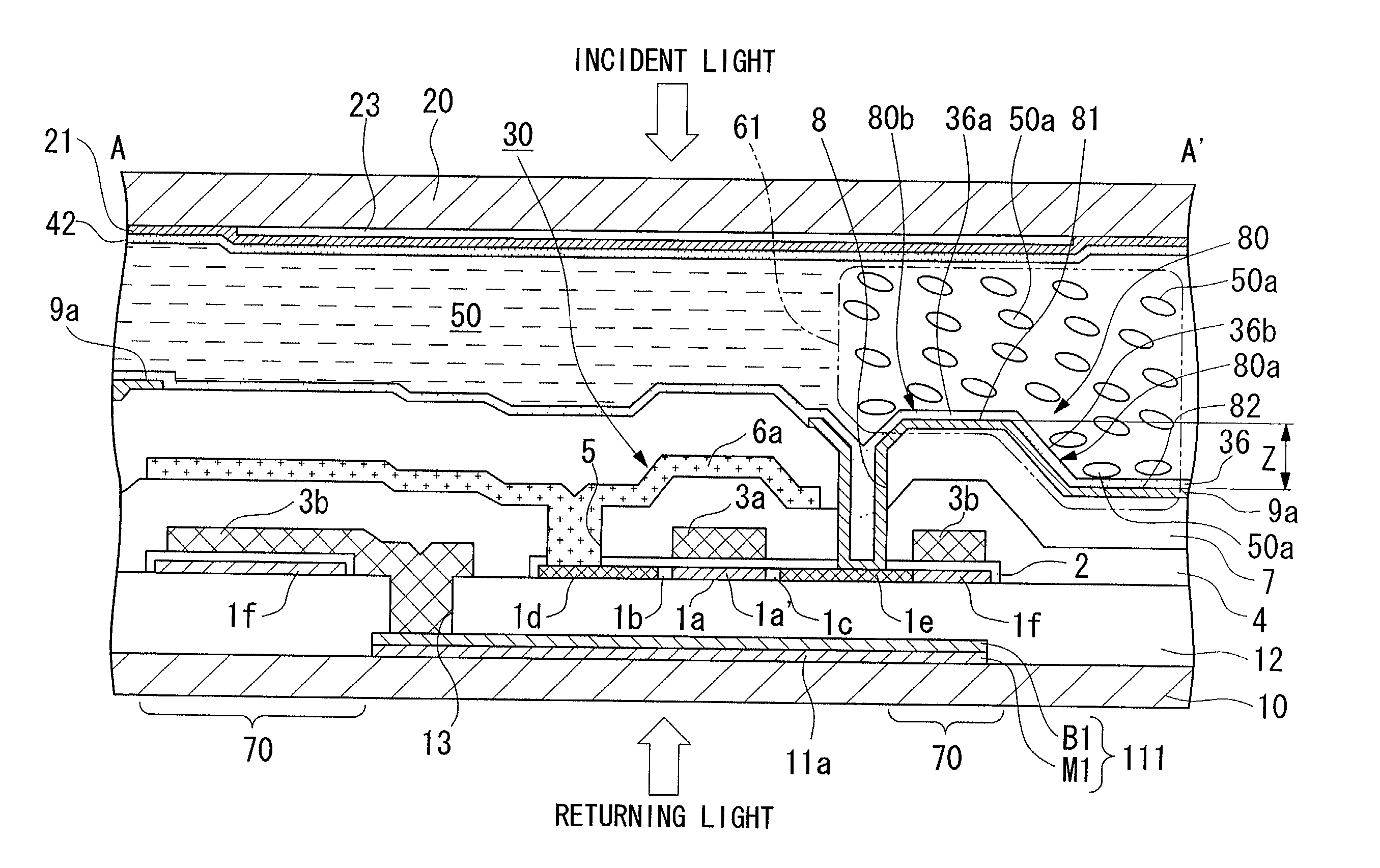
[0017] Also, an object of this invention is to provide a liquid crystal device by which inferior evaporation areas of inorganic materials is not generated near the gap section of the underlayer of the alignment layer even if pixel elements are as fine as 20 .mu.m or less, to prevent the occurrence of inferior alignment of the liquid crystals due to the irregularities in the alignment layer due to inferior evaporation areas of inorganic material, and to reduce the occurrence of inferior display. A manufacturing method for a substrate for such a liquid crystal device is another object of the present invention.

Problems solved by technology

However, for example, if the pixel pitch becomes as fine as 20 .mu.m, there will be areas where effective rubbing treatment on the alignment layer is impossible because of the gap section on the underlayer of the alignment layer in the case of liquid crystal light valve in which an alignment layer made of an organic layer such as polyimide is provided; thus, disclination of the liquid crystal occurs nearby sometimes degrading display quality.
Such a problem becomes more apparent if the pixel pitch is made finer.
Thus, the orientation of the liquid crystal molecules lose uniformity, the contrast of the display decreases, and sometimes ultimately leads to inferior display quality.
The reasons such problems occur is that the organic layer made of polyimide absorbs some amount of the 400 to 450 nm wavelength visible light, the alignment layer deteriorates due to the absorption of the light, the orientations of the liquid crystal lose alignment uniformity near the deteriorated area of the alignment layer, and thus degraded display quality results.
However in contrast to advantages such as light resistance and heat resistance, an alignment layer made of an inorganic layer has disadvantages such as weak alignment uniformity of liquid crystals as compared to an alignment layer made of an organic layer.
Accordingly, in a liquid crystal device using an inorganic alignment layer, disclination easily occurs if any factor occurs causing loss of alignment uniformity of the liquid crystals; inferior display is provided.
Such irregularities in the surfaces produce shadows on the substrate during oblique evaporation; thus, defective parts may sometimes be generated on the alignment layer.
However, the aligning uniformity of the inorganic evaporation layer is so weak that disclination may be caused.
Because of this tendency, inferior display such as one in which there is light leakage in the domain in which the alignment direction is different occurs, and the display quality decreases due to low contrast.
However, if the pre-tilt angle is increased in the case of an inorganic alignment layer in which the aligning uniformity was originally weak, the spiral structure of the liquid crystals between the substrates becomes unstable.
Therefore, inferior display is produced due to the existence of reverse twist domains which are areas in which the twisting directions of liquid crystals becomes partially opposite.
This problem also occurs in liquid crystal devices using alignment layers made of an inorganic oblique evaporation layer formed on the underlayer on which surface the gap section exists.
Above problem is not limited to the case of an active matrix type liquid crystal device using a 3-terminal-type-element such as a TFT element; but it is a common problem among active matrix type liquid crystal devices using 2-terminal-type-elements such as a Thin-Film-Diode (hereinafter called TFD) and passive matrix type liquid crystal devices whenever an inorganic alignment layer is used in the liquid crystal device.
The reason is that the evaporation is hardly possible in the area shaded by the gap section on the surface of the underlayer of the alignment layer; thus, such area becomes a evaporation defect area when an element substrate on which a plurality of wiring and a plurality of insulating layers are formed is fixed at a certain angle and then forming an alignment layer by unidirectional evaporation of an inorganic material.
If the thickness of the first inorganic oblique evaporation layer is less than 5 nm, the pre-tilt angle is not arranged for the liquid crystal molecule, and such a condition may cause disclination.
If the deposition angle of the oblique evaporation direction in the first oblique evaporation from the substrate is less than 5 degrees, the density of the columnar structure formed is too low; thus the alignment direction of the liquid crystal molecules becomes unstable, and the alignment uniformity inside the plane along the inside plane direction of the substrate is lost.
If the deposition angle of oblique evaporation direction from the substrate is larger than 10 degrees, the density of the columnar structure formed becomes high, and the effect that the gap of the columnar structure of the first inorganic oblique evaporation layer is filled by the columnar structure of the second inorganic oblique evaporation layer can hardly be obtained; thus, as a result, the area where there is no pre-tilt in the alignment of liquid crystal molecule expands when manufacturing the liquid crystal device with this substrate.
If the thickness of the first inorganic oblique evaporation layer is less than 5 nm, a pre-tilt angle is not provided to the liquid crystal molecules, and such a condition may cause disclination.

Method used


Image

  • Liquid crystal device, projection display device and, manufacturing method for substrate for liquid crystal device
  • Liquid crystal device, projection display device and, manufacturing method for substrate for liquid crystal device
  • Liquid crystal device, projection display device and, manufacturing method for substrate for liquid crystal device

Examples


experimental example 1

[0196] The liquid crystal device of above first embodiment which is provided with the alignment layer made of two layers of inorganic oblique evaporation layer was produced. The pre-tilt angle .theta. was varied to various values by controlling the evaporation conditions while the cell gap d was made to be 3 .mu.m, and the twist angle .phi. of the liquid crystal layer was 90 degrees. The value of the helical pitch P of the liquid crystal was changed to 30, 15, 10, 7.5 (.mu.m) by adjusting the amount of chiral complex which is added to the raw material for liquid crystal. The existence of defective alignment was detected on the display of an actual projection type display device by visual observation under condition that the pre-tilt angle .theta. is 8 degrees. The results are shown in TABLE 1.

1TABLE 1 P(.mu.m) d / P(-) Display Condition 30 0.1 A 15 0.2 O 10 0.3 O 7.5 0.4 B

[0197] In TABLE 1, "A" in "Display Condition" indicates the case in which the area in which the twist angle is 90 ...

experimental example 2

[0199] The liquid crystal device of the second embodiment in which the alignment layer made of a single layer of inorganic oblique evaporation layer was produced. The pre-tilt angle .theta. was varied to various values by controlling the evaporation conditions while the cell gap d is made to be 3 .mu.m, and the twist angle .phi. of the liquid crystal layer is 90 degrees. The value of the helical pitch P of the liquid crystal was changed to 20, 12, 8.6, 6.7 (.mu.m) by adjusting the amount of chiral complex which is added to the raw material for liquid crystal. The existence of defective alignment was detected on the display of actual projection type display device by visual observation under conditions in which the pre-tilt angle .theta. was 27 degrees. The results are shown in TABLE 2.

2TABLE 2 P(.mu.m) d / P(-) Display Condition 20 0.15 C 12 0.25 O 8.6 0.35 O 6.7 0.45 B

[0200] In TABLE 2, "A" in "Display Condition" indicates the case in which the area in which the twist angle is 90 deg...

experimental example 3

[0202] Also, the inventors of the liquid crystal device of the present invention performed an experiment for proving the effect of the liquid crystal device in the present invention. The result of the experiments are explained as follows.


PUM

PropertyMeasurementUnit
twist angleaaaaaaaaaa
azimuth anglesaaaaaaaaaa
thicknessaaaaaaaaaa

Abstract

A liquid crystal device has inorganic alignment layers (36, 42) disposed on a surface of a liquid crystal layer side of a pair of the substrates, when the range of the average pre-tilt angle theta of liquid crystal molecules 50a of the liquid crystal layer is 5 degrees<=theta<=20 degrees, twist angle phi of the liquid crystal molecules (50a) of the liquid crystal layer, cell gap d, and helical pitch P of the liquid crystal molecules of the liquid crystal layer satisfy the relationship of (0.6 / 360)phi<d / P<(1.4 / 360)phi, and when the range of the average pre-tilt angle theta of liquid crystal molecules 50a of the liquid crystal layer is theta>20 degrees, twist angle phi of the liquid crystal molecules (50a) of the liquid crystal layer, cell gap d, and helical pitch P of the liquid crystal molecules of the liquid crystal layer satisfy the relationship of (0.8 / 360)phi<d / P<(1.6 / 360)phi.

Description

[0001] 1. Field of the Invention[0002] The present invention relates to liquid crystal devices, projection display devices, and manufacturing methods for substrates for liquid crystal devices. This invention particularly relates to the construction of desirable liquid crystal devices to be used as a light source for a liquid crystal projector, and to a manufacturing method for a substrate for a liquid crystal device.[0003] 2. Description of Related Art[0004] For a projection liquid crystal display device, such as a liquid crystal projector, there is the three-panel type in which three liquid crystal panels corresponding to the three primary colors red (R), green (G), and blue (B) are used, and the one-panel type in which one liquid crystal panel and a color generating device are used. For a liquid crystal light source which is a part of such a projection liquid crystal display device, active matrix type liquid crystal panels are typically used.[0005] Also, a liquid crystal panel com...

Claims


Application Information

Patent Timeline
Patent Type & Authority Applications(United States)
IPC IPC(8): G02F1/1337G02F1/13
CPCG02F1/133734G02F1/133753G02F1/13
Inventor TANAKA, TAKAAKIYAMAZAKI, YASUSHI
Owner SEIKO EPSON CORP
Learn More