Liquid crystal display device having an auxiliary wiring

Inactive Publication Date: 2003-01-23
INNOLUX CORP
View PDF6 Cites 10 Cited by
  • Summary
  • Abstract
  • Description
  • Claims
  • Application Information

AI Technical Summary

Problems solved by technology

Therefore, the metallic part can suffer some damage due to its contact with the probe, so that the damage may promote metallic corrosion to lead influence such as deterioration of electrical conductivity of the bus-line.
Accordingly, it has to always provide a bus-line to be monitored in waveform with a contact pad, and even when all the bus-line

Method used


Image

  • Liquid crystal display device having an auxiliary wiring
  • Liquid crystal display device having an auxiliary wiring
  • Liquid crystal display device having an auxiliary wiring

Examples


Example

[0031] [Embodiment 1]

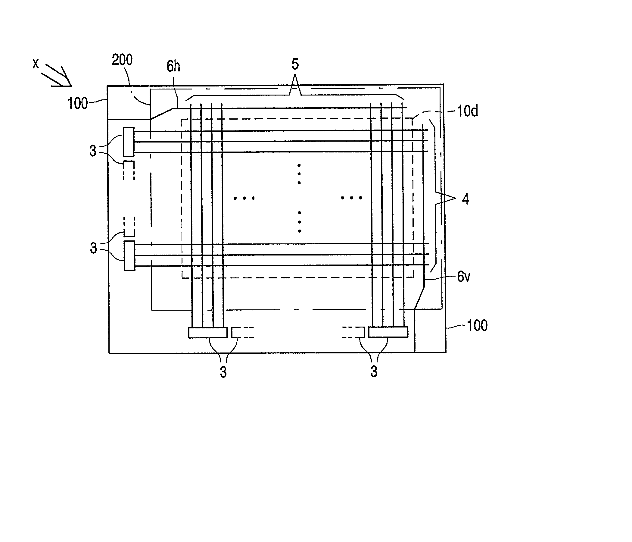
[0032] FIG. 1 schematically shows in a plan view a configuration of one substrate assembly 100 used in one embodiment of liquid crystal display device according to the invention.

[0033] It should be noted that: although the one substrate assembly 100 is assembled with another substrate assembly 200 with being faced to each other and a liquid crystal medium is encapsulated between them to finally make a liquid crystal display device (panel), especially the one substrate assembly's configuration will be described hereinafter for clarity of the explanation.

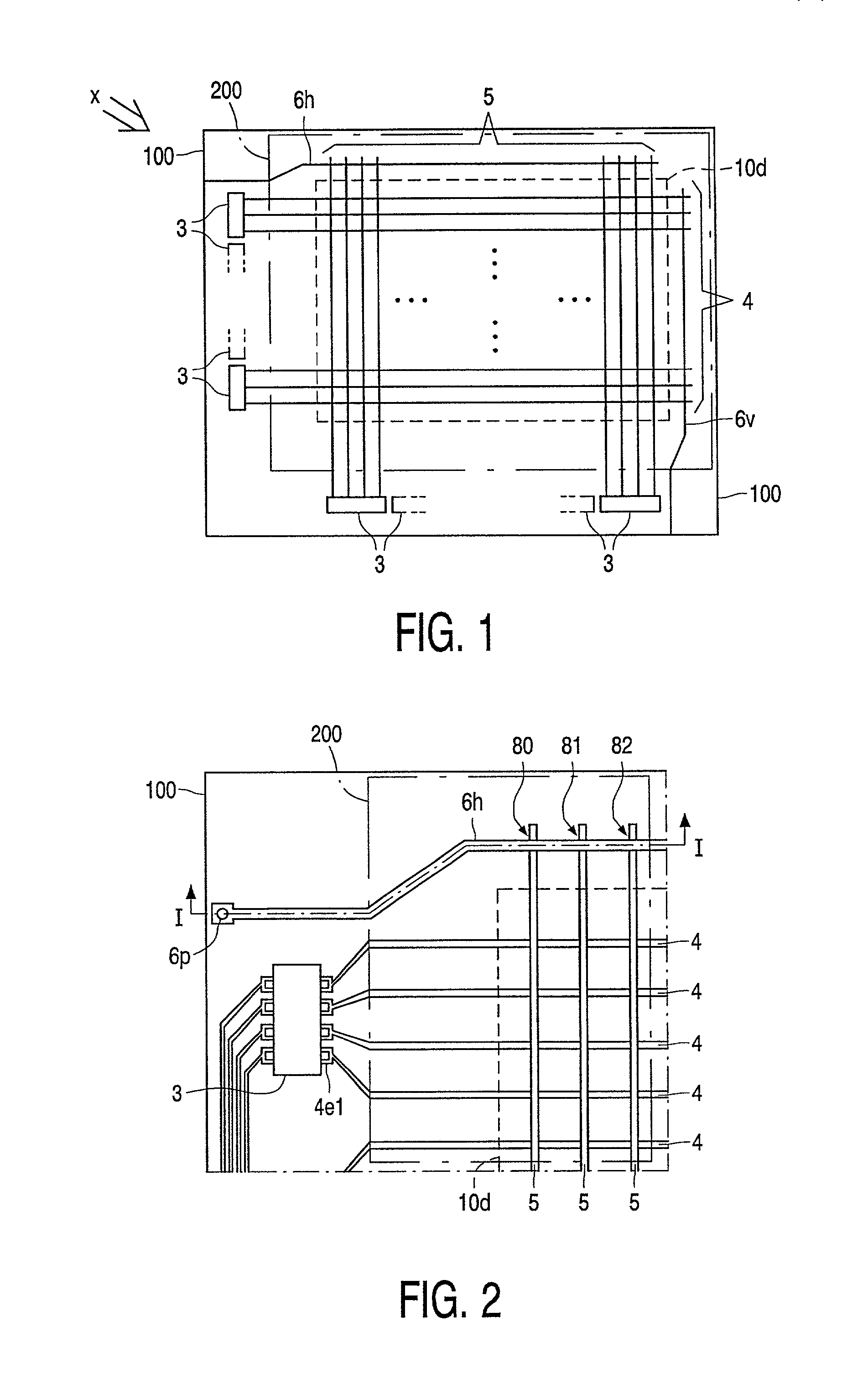
[0034] In FIG. 1, a predetermined display area 10d is defined in a substrate body (description later) of the substrate assembly 100, wherein images to be displayed are formed. The substrate assembly 100 is provided with two series of bus-lines 4 and 5 which are arranged to extend orthogonally to each other over the display area 10d. The one series of bus-lines 4 horizontally run in parallel from one edge side of t...

Example

[0054] [Embodiment 2]

[0055] FIG. 4 schematically shows in a plan view an arrangement of one substrate assembly and the surrounding parts combined with it, which are used in a liquid crystal display device according to another embodiment of the present invention.

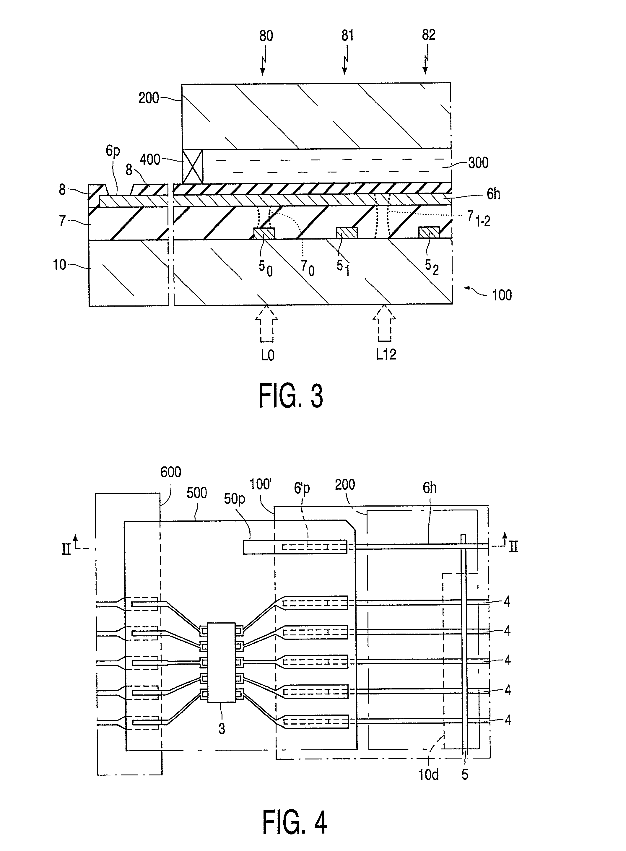
[0056] In a substrate assembly 100' in FIG. 4, the driver ICs 3 are connected to the bus-lines 4 and 5 by means of TAB (Tape Automated Bonding) style. Therefore, as also seen from FIG. 5 that shows a II-II sectional view of FIG. 4, the auxiliary wiring pattern 6h has a pattern shape and a coupling portion 6p', which are suitable to be coupled at its end portion with an extension wiring pattern 50p formed on a TAB tape 500.

[0057] The driver ICs 3 are mounted on the TAB tape 500 on which their respective connecting patterns are formed for terminals of the ICs. These connecting patterns form connecting pads at edge portions on both the right and left sides of the tape 500, the pads being for connection of one ends of the bus-lin...

Example

[0060] [Embodiment 3]

[0061] FIG. 6 schematically shows in a plan view an arrangement of one substrate assembly and the surrounding parts combined with it, which are used in a liquid crystal display device according to a further embodiment of the present invention.

[0062] The substrate assembly 100' in FIG. 6 is also intended to connect the driver ICs 3 to the bus-lines 4 and 5 in the TAB scheme, for the purpose of which it has a coupling portion 6p' similar to that in FIG. 5.

[0063] However, the TAB tape 500' has an extension wiring pattern 50f that extends longer than the above-mentioned extension wiring pattern 50p further up to the print board 600'. The extension wiring pattern 50f connects to the coupling portion 6p'. The print board 600' is provided at its edge side with a probe pad 60p different from a connecting pad led from a connecting pattern for a circuit mounted on the print board 600'. The extension wiring pattern 50f is made contact with the connecting pad 60p, e.g. by m...


PUM


Abstract

To enable freely choose a bus-line to be monitored without such a problem that the bus-line is made corroded. A liquid crystal display device comprising: a substrate (10) in which a display area (10d) is delimited; and two series of bus-lines (4, 5) supported by the substrate, one ends of the bus-lines being located in proximity to one side of the display area, another ends of the bus-lines being located in proximity to another side of the display area which is opposite to the one side of the display area, the two series of bus-lines (4, 5) being arranged to extend over the display area in such a manner that the one series of bus-lines (4) is orthogonal to the other series of bus-lines (5). The display device further comprises: a conductive auxiliary wiring pattern (6h, 6v) which extends in such a manner that the pattern crosses another end(s) of the bus-line(s), which is/are all to be monitored, of the one series of bus-lines (4 or 5) via an electrically insulating layer (7), and which is led out to a predetermined location on a side of one ends of the bus-lines (5 or 4) of the other series to form a coupling portion (6p) capable of electrically connecting to the exterior.

Description

[0001] 1. Field of the Invention[0002] The present invention relates to a liquid crystal display device. The invention relates, in particular to a liquid crystal display device having an auxiliary wiring pattern that can make electric characteristics to be observed. The invention also relates to a method of monitoring electric characteristics of bus-lines of a liquid crystal display device by using s[0003] 2. Description of Related Art[0004] Such a type of liquid crystal display device is disclosed in, e.g. a reference of Japanese Patent Application Laid-Open No. 233,514 / 92 (or the corresponding application, U.S. Pat. No. 5,349,226).[0005] In this reference, there is described a liquid crystal display device having an active matrix board provided with an array of thin film transistors formed in matrix on an insulative substrate, wherein portions of gate bus-line and source bus-line of the thin film transistor array form contact pads for probing of which metallic parts are exposed to...

Claims


Application Information

Patent Timeline
IPC IPC(8): G02F1/13G02F1/1345G02F1/1362
CPCG02F1/1309G02F1/1345G02F2001/136254G02F1/136254
Inventor HASHIMOTO, KAZUYA
Owner INNOLUX CORP
Why Eureka
Try Eureka