
Coated silicon wafer and process for its production

a technology of silicon wafers and coatings, applied in the direction of crystal growth processes, basic electric elements, electrical equipment, etc., can solve the problems of unable to predict, produce wafers, and lose corresponding components,

Inactive Publication Date: 2003-03-06
WACKER SILTRONIC
View PDF5 Cites 17 Cited by
  • Summary
  • Abstract
  • Description
  • Claims
  • Application Information

AI Technical Summary

Benefits of technology

[0028] However, if it is appropriate for an etching step to be carried out, wet-chemical etching using an acidic etching mixture and a removal of 3 .mu.m to 30 .mu.m of silicon is preferred. If a silicon wafer with a concave thickness distribution has already been produced in the abrasive step of the process according to the invention, the etching step may be carried out in accordance with the prior art, for example as described in DE 199 33 257 C1. This uses the rotary principle with gas being fed in while maintaining the predetermined wafer geometry. However, within the context of the invention it is also possible for the concave thickness distribution of the silicon wafers to be produced for the first time in the etching step or to be enhanced in the etching step. There are various possibilities in this respect, defined by the choice of process parameters; their effect on the wafer geometry is in this case generally determined by processing and measuring test wafers. This leads to an optimized set of parameters which results in etched wafers with a defined concave thickness distribution. In the case of the preferred acid etching process, it is possible to produce concave wafers for example by reducing the dissipation of heat or reducing the quantity of gas which is fed in.
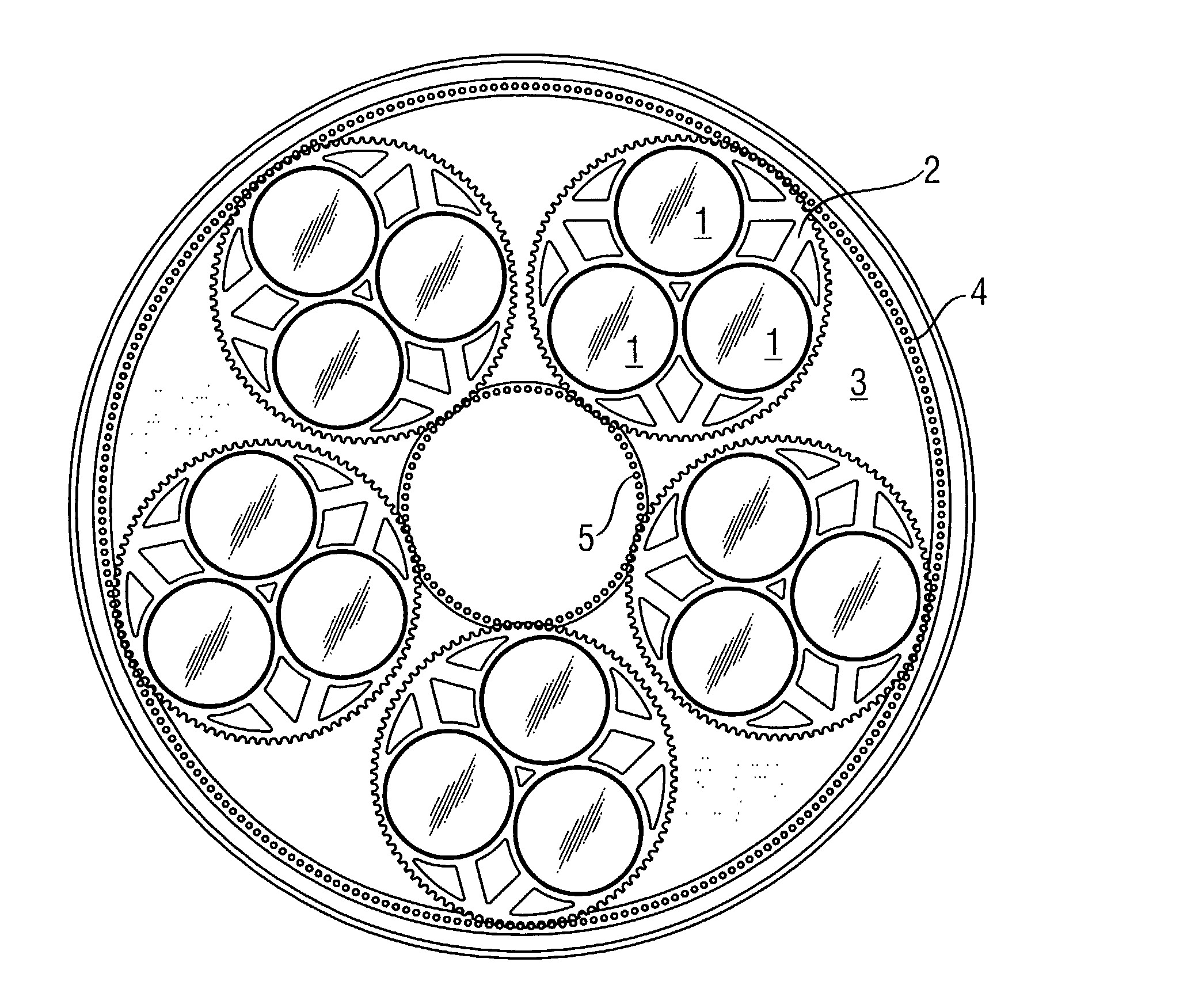
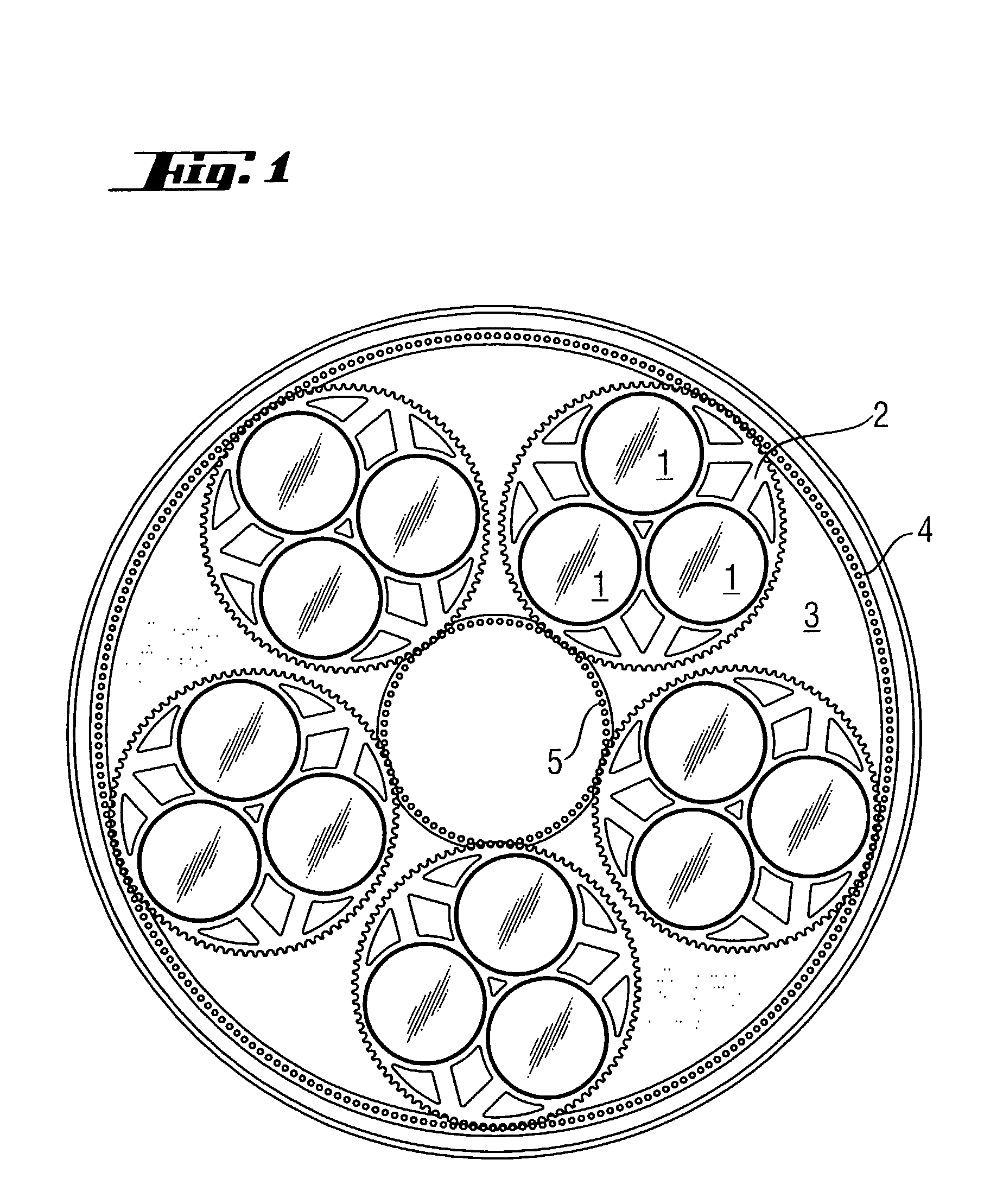
[0030] At this point in the process sequence, it is preferable to form groups of silicon wafers which are simultaneously subjected to double-side polishing. Depending on the size and occupancy of the polishing machine, these groups may, for example, be 15 or 30 wafers with a diameter of 200 mm or 5 or 15 wafers with a diameter of 300 mm or 3 or 5 wafers with a diameter of 450 mm. It is possible for the wafers to be grouped without measurements if the thickness and shape are very highly constant. However, to ensure robust process management in everyday operation, a sorting station is generally required. This sorting station is equipped with a measuring unit for determining wafer thickness and shape and a sorting unit having at least one entry station and a plurality of exit stations for cartridges for holding the sorted silicon wafers. The wafers are then brought together for a polishing run in such a manner that (a) the difference between center thickness and edge thickness of the wafers. These wafers preferably have a concavity of 1 .mu.m to 10 .mu.m, which differs by preferably less than or equal to 3 .mu.m, particularly preferably by less than or equal to 2 .mu.m, for example 4 .mu.m.+-.1 .mu.m. Also (b) the mean thickness of the silicon wafers differs within a thickness range of preferably less than or equal to 3 .mu.m and particularly preferably less than or equal to 2 .mu.m, for example within .+-.1 .mu.m. If the process steps which have been described hitherto are carried out correctly, this sorting is possible virtually without losses of wafers as a result of extreme shape and thickness data.

Problems solved by technology

If this value is exceeded, the stepper has focusing problems and therefore the corresponding component is lost.
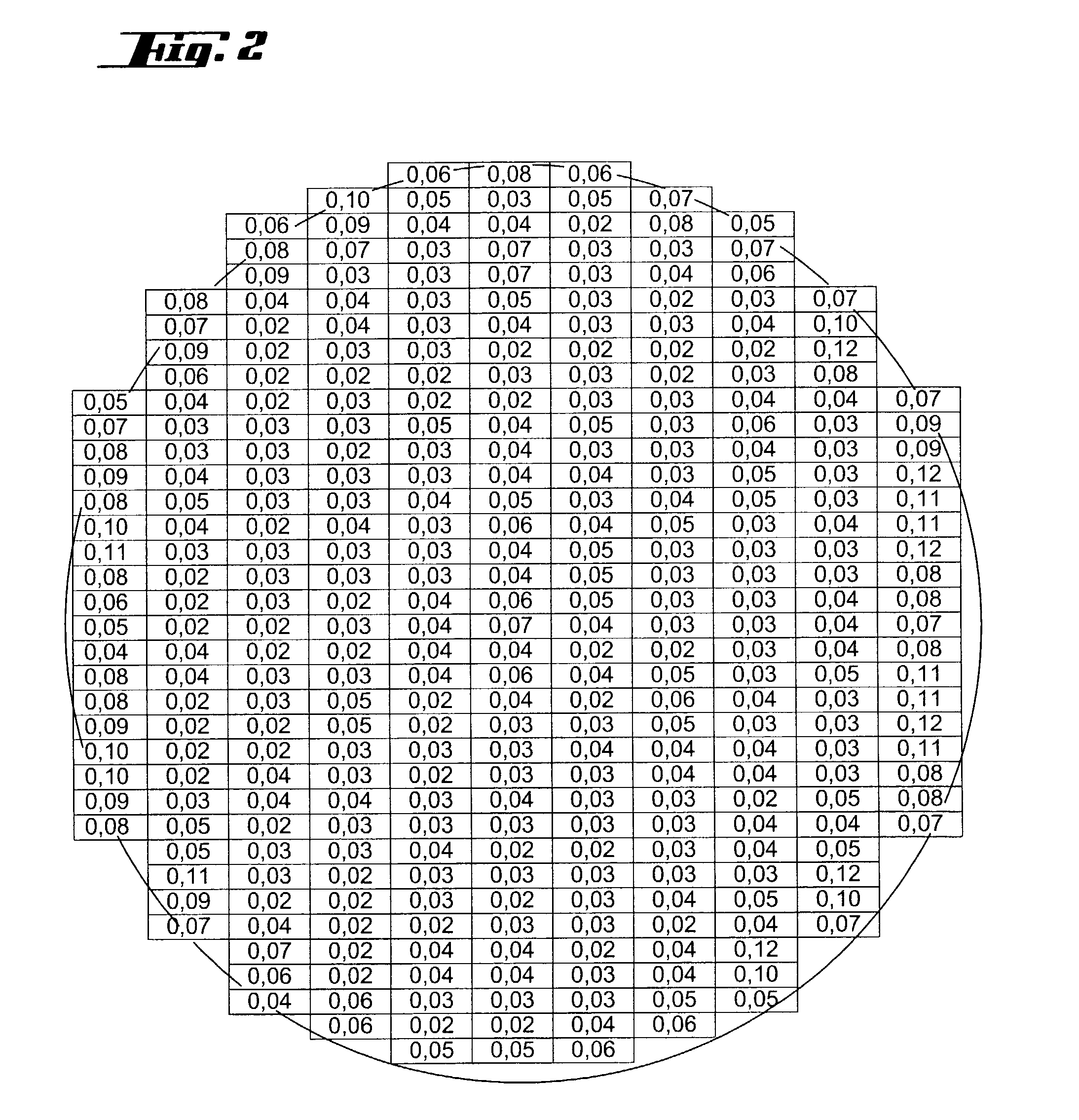
However, according to the prior art it is impossible to produce wafers which after, application of the coating have SFQR.sub.max values of less than or equal to 0.10 .mu.m and therefore are suitable as starting material for the fabrication of components used in the 0.10 .mu.m technology, in economically viable yields.
The discovery of the claimed narrow window for the abovementioned variables is the result of extensive tests carried out on an operational scale, the results of which were unexpectedly surprising and impossible to predict.

Method used


Image

  • Coated silicon wafer and process for its production
  • Coated silicon wafer and process for its production
  • Coated silicon wafer and process for its production

Examples


example

[0057] The procedure was as in the Comparative Example, with the following differences:

[0058] (1) The grinding process was carried out in such a way that a concave thickness distribution was produced by inclining the axis of rotation of the grinding wheel with respect to that of the wafer holder.

[0059] (2) Before the double-side polishing, the silicon wafers were divided into groups of 15 wafers which were to be polished simultaneously and in which the thickness difference between wafer edge and wafer center within each group was 4 .mu.m.+-.1 .mu.m.

[0060] (3) During the sorting into groups, account was also taken of the fact that the distribution (in accordance with the Comparative Example) of the mean thicknesses of the silicon wafers within each group was .+-.1 .mu.m. Overall, therefore, four thickness groups were produced ([802.+-.1] .mu.m; [804.+-.1] .mu.m; [806.+-.1] .mu.m; [808.+-.1] .mu.m).

[0061] (4) For the double-side polishing, carriers with a thickness of 773 .mu.m were u...


PUM

PropertyMeasurementUnit
thicknessaaaaaaaaaa
diameteraaaaaaaaaa
flatnessaaaaaaaaaa

Abstract

A silicon wafer is provided having a polished front surface with an epitaxial coating and a polished back surface, which is distinguished by a SFQRmax value of less than or equal to 0.10 mum (26 mmx8 mm; 99%). There is also a process for producing silicon wafers of this type by sawing up a single crystal, carrying out an abrasive step, simultaneously polishing a front surface and a back surface of at least three silicon wafers, and applying an epitaxial coating. This process includes the following conditions being satisfied simultaneously: (a) before the simultaneous polishing, the silicon wafers have a concave thickness distribution, the center thickness being 1 mum to 10 mum lower than the edge thickness, and this thickness difference differing by less than or equal to 3 mum within one polishing run; (b) the mean thickness of the silicon wafers prior to the simultaneous polishing differs by less than or equal to 3 mum within one polishing run; and (c) the thickness of the carriers used during the simultaneous polishing is 1 mum to 5 mum lower than the thickness of the finished polished silicon wafers.

Description

[0001] 1. Field of the Invention[0002] The present invention relates to a silicon semiconductor wafer which has been epitaxially coated on the front surface and has an improved flatness, and to a process for producing a wafer of this type. Epitaxially coated silicon wafers with a very high flatness are suitable for use in the semiconductor industry, in particular for the fabrication of electronic components with line widths of less than or equal to 0.10 .mu.m.[0003] 2. The Prior Art[0004] A silicon wafer which is suitable in particular for the fabrication of electronic components with line widths of less than or equal to 0.10 .mu.m, generally referred to as the 0.10 .mu.m technology generation, must have a large number of particular properties. In this context, one critical property is its local flatness. The modern stepper technology requires optimum local flatnesses in all subregions of a surface of the wafer, expressed, for example, as SFQR (site front-surface referenced least sq...

Claims


Application Information

Patent Timeline
Patent Type & Authority Applications(United States)
IPC IPC(8): C30B25/02C30B33/00H01L21/02H01L21/304H01L21/205
CPCC30B25/02C30B29/06C30B33/00
Inventor WENSKI, GUIDOMARECK, UTEALTMANN, THOMAS
Owner WACKER SILTRONIC
Learn More