
Semiconductor device and method of making the same

a semiconductor and chip technology, applied in the direction of semiconductor devices, semiconductor/solid-state device details, electrical equipment, etc., can solve the problems of chip electrode damage, adhesive sealing cracks and/or release from the substrate and/or the chip, and solder bumps that cannot be expected to be detached from the electrodes

Inactive Publication Date: 2003-03-13
FUJITSU LTD
View PDF6 Cites 5 Cited by
  • Summary
  • Abstract
  • Description
  • Claims
  • Application Information

AI Technical Summary

Benefits of technology

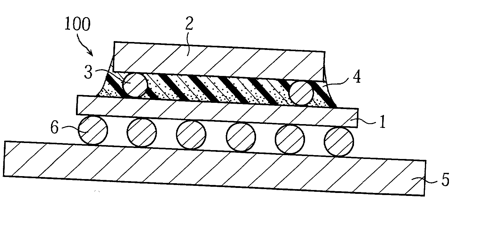
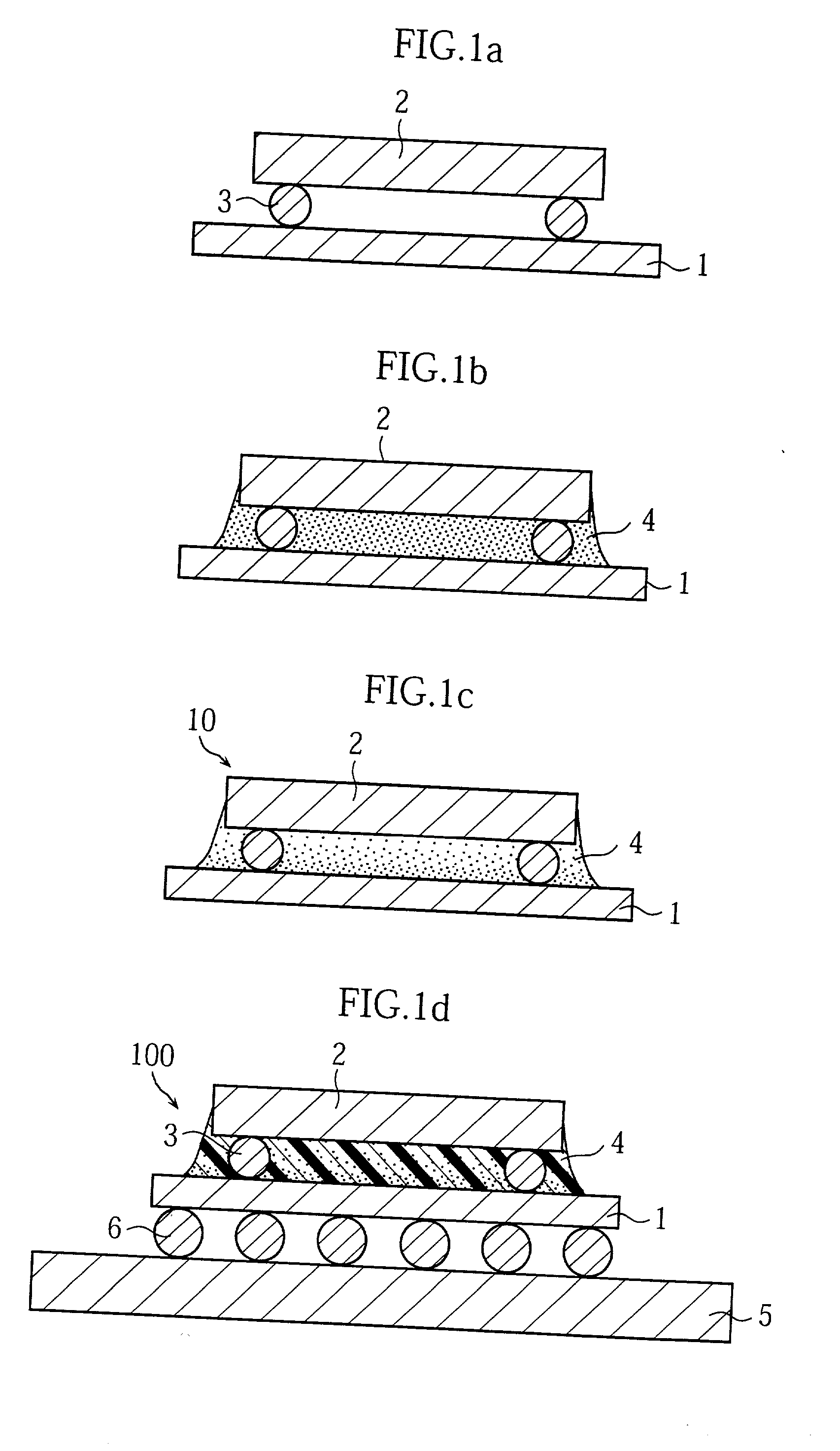
[0009] With this method, the reliability of the bond between the semiconductor chip and the substrate does not deteriorate in mounting the substrate to a mother board by reflow soldering. The sealing adhesive composition for sealing between the semiconductor chip and the substrate hardens in two stages. Specifically, the first main ingredient of the sealing adhesive composition undergoes the primary hardening before bonding the substrate (i.e., the bonded assembly of the semiconductor device and the substrate) onto the mother board, thereby protecting the flip-chip bond. Herein, the primary hardening means the state where the hardening reaction occurs with respect to the first main ingredient but hardly occurs with respect to the second main ingredient which therefore retains its uncured state. Then, due to the heat of reflow soldering for mounting the chip-substrate assembly to the mother board, the adhesive sealing undergoes the secondary hardening. Specifically, the uncured second main ingredient of the sealing adhesive composition first softens upon heating, so that the entire adhesive sealing softens once, followed by the secondary hardening of the second main ingredient. During the preliminary softening of the adhesive sealing, the thermal stresses previously generated at the adhesive sealing after the primary hardening are relieved. Therefore, in the reflow soldering, undesirable stress is not transmitted from the adhesive sealing to the substrate or the semiconductor chip. Thus, it is possible to prevent unexpected removal of the adhesive sealing from the substrate or the semiconductor chip.
[0010] According to the prior art, the adhesive sealing provided at the flip-chip bonded portion is completely hardened by heat before the chip-substrate assembly is mounted to a motherboard. Therefore, when the adhesive sealing is subjected to a high temperature during the reflow soldering for mounting the chip-substrate assembly to the mother board, the adhesive sealing may be removed from the substrate or the semiconductor chip due to the thermal stresses generated in the adhesive sealing. According to the present invention, on the other hand, the secondary hardening of the adhesive sealing occurs during the heating for reflow soldering so that the thermal stresses generated in the adhesive sealing can be relieved. Thus, the present invention can prevent the above-described drawbacks of the prior art.
[0013] Preferably, the sealing adhesive composition exhibits at least two peak temperatures in differential scanning calorimetry. More preferably, the sealing adhesive composition includes a lower peak temperature lying in a range of 110-170.degree. C. and a higher peak temperature lying in a range of 180-240.degree. C. Such peak temperature setting makes it possible to perform the two-stage hardening of the adhesive sealing in an appropriate manner.
[0017] For improving affinity between the inorganic filler and the resin ingredients, the sealing adhesive composition may further contain a coupling agent. Examples of the coupling agent include vinyltrichlorosilane, vinyl tris-(2-methoxyethoxy) silane, .gamma.-methacryloxypropyl trimethoxy silane, .gamma.-methacryloxypropyl triethoxy silane, .beta.-(3,4-epoxycyclohexyl) ethyl trimethoxy silane, .gamma.-glycidoxypropyl trimethoxy silane, .gamma.-glycidoxypropyl triethoxy silane, .gamma.-chloropropyl trimethoxy silane, .gamma.-mercaptopropyl trimethoxy silane, .gamma.-aminopropyl triethoxy silane, N-phenyl-.gamma.-aminopropyl trimethoxy silane, N-.beta.-aminoethyl-y-aminopropyl trimethoxy silane, and N-.beta.-aminoethyl-.gamma.-aminopropyl methyl dimethoxy silane.
[0021] According to the third aspect, the adhesive sealing comprises a first portion containing the inorganic filler at a higher density and thereby having a higher modulus of elasticity, and a second portion containing the inorganic filler at a lower density and thereby having a lower modulus of elasticity. Therefore, in the reflow heating, the second portion having a lower modulus of elasticity serves as a cushion for alleviating stresss applied from the adhesive sealing toward the semiconductor chip. As a result, the breakage of the bond between the chip electrodes and the bumps can be prevented, thereby providing a high bonding reliability of the semiconductor chip relative to the substrate.

Problems solved by technology

However, a substrate of these kinds differs largely from an LSI chip in coefficient of thermal expansion, which may lead to the generation of large thermal stresses and thereby result in unexpected detachment of solder bumps from the electrodes of the substrate and / or the electrodes of the chip.
As a result, the adhesive sealing may suffer cracks and / or release from the substrate and / or the chip due to the deformation of the LSI chip and the substrate or due to thermal stresss generated in the adhesive sealing.
This may lead to removal of the solder bumps or pins, which may, in turn, cause damage to the chip electrodes.
Such a damage is remarkable at the electrodes provided at a peripheral portion of the LSI chip, because the LSI chip warps largely at the peripheral portion.
This may cause adjacent bumps to be electrically connected to each other to result in shorting of the bumps.
In this way, the prior art methods for making a semiconductor device are still insufficient in terms of the bonding reliability between the LSI chip and the substrate.
Therefore, in the reflow soldering, undesirable stress is not transmitted from the adhesive sealing to the substrate or the semiconductor chip.

Method used


Image

  • Semiconductor device and method of making the same
  • Semiconductor device and method of making the same

Examples


example 2

[0041] A sealing adhesive composition was prepared in a manner similar to Example 1. The difference of the sealing adhesive composition of Example 2 from that of Example 1 lies in that the proportion of bisphenol F resin (EXA-830 available from Dainippon Ink and Chemicals, Incorporated) was reduced to 75 parts by weight, while 25 parts by weight of naphthalene resin (HP4032D available from Dainippon Ink and Chemicals, Incorporated) was further added as a third main resin ingredient. Subsequently, in a manner similar to Example 1, the differential scanning calorimetry and the measurement of glass transition point, gel time and viscosity were performed. Further, samples of chip-substrate assembly each including an adhesive sealing formed of this resin composition were prepared and checked for thermal stress influences, settlement of inorganic filler, temperature cycle resistance and humidity resistance, in the same manner as in Example 1.

[0042] In the differential scanning calorimetry...

example 3

[0043] A sealing adhesive composition was prepared in a manner similar to Example 1. The difference of the sealing adhesive composition of this Example from that of Example 1 lies in that the proportion of bisphenol F resin (EXA-830 available from Dainippon Ink And Chemicals, Incorporated) was reduced to 50 parts by weight, while 50 parts by weight of naphthalene resin (HP4032D available from Dainippon Ink And Chemicals, Incorporated) was further added as a third main ingredient. Subsequently, in a manner similar to Example 1, the differential scanning calorimetry and the measurement of glass transition point, gel time and viscosity were performed. Further, samples of chip-substrate assembly each including an adhesive sealing formed of this resin composition were prepared and checked for thermal stress influences, settlement of inorganic filler, temperature cycle resistance and humidity resistance, in the same manner as in Example 1.

[0044] In the differential scanning calorimetry, t...


PUM

PropertyMeasurementUnit
peak temperatureaaaaaaaaaa
temperatureaaaaaaaaaa

Abstract

According to a method of making a semiconductor device, a semiconductor chip is bonded to a substrate via bumps by flip-chip bonding. Then, a sealing adhesive composition is loaded between the semiconductor chip and the substrate to provide an adhesive sealing. The sealing adhesive composition, which is capable of hardening in two stages, contains at least a first main resin ingredient, a second main resin ingredient and a hardening agent. Then, the adhesive sealing is heated for primary hardening. Then, the substrate is placed on a mother board with a solder material interposed between the substrate and the mother board. Finally, the adhesive sealing is heated for secondary hardening while the solder material is reflowed for bonding the substrate to the mother board.

Description

BACKGROUND OF THE INVENTION 1. Field of the Invention[0001] The present invention relates to a method of making a semiconductor device of the type which comprises a semiconductor chip bonded to a substrate by flip-chip bonding with an adhesive sealing interposed between the semiconductor chip and the substrate. The present invention also relates to a semiconductor device made by such a method. 2. Description of the Related Art[0002] In a semiconductor device for use in a high-end apparatus such as a super computer, an LSI chip is bonded to an MCM (Multi-Chip Module) substrate by flip-chip bonding using solder bumps for realizing a high performance and high-density mounting. Generally, in the flip-chip bonding, a gap between the LSI chip and the MCM substrate is sealed with a resin for preventing air or dust from entering the gap.[0003] Recently, the flip-chip bonding is increasingly utilized also for making a semiconductor device for use in a middle-end or low-end apparatus. In such...

Claims


Application Information

Patent Timeline
Patent Type & Authority Applications(United States)
IPC IPC(8): H01L21/60H01L21/56H01L23/12H01L23/498
CPCH01L21/563H01L23/49816H01L2924/01006H01L2224/32225H01L24/29H01L2924/15311H01L2924/09701H01L2924/01082H01L2924/01075H01L2924/0105H01L2924/01047H01L2924/01033H01L2924/01029H01L2924/01027H01L2924/01005H01L2924/01004H01L2224/92125H01L2224/16225H01L2224/73203H01L2224/73204H01L2224/83102H01L2924/00H01L2924/3512H01L2924/15787H01L2924/351H01L23/12
Inventor YAGI, TOMOHISAIMAIZUMI, NOBUHIROUSUI, YASUHIROFUKUZONO, KENJI
Owner FUJITSU LTD
Learn More