

Electron-emitting device and image-forming apparatus
a technology of electron-emitting device and image-forming apparatus, which is applied in the manufacture of electric discharge tubes/lamps, tubes with screens, discharge tubes luminescnet screens, etc., and can solve the problems of inability to make small beams, limited lifetime of fe-type devices, and inducing the thermal destruction of electron-emitting portions
- Summary
- Abstract
- Description
- Claims
- Application Information
AI Technical Summary
Problems solved by technology
Method used
Image

Examples
embodiment 1
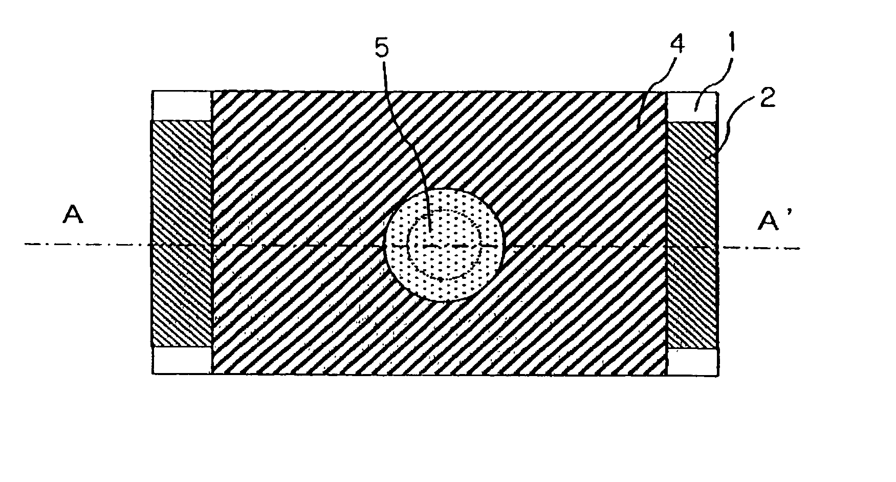
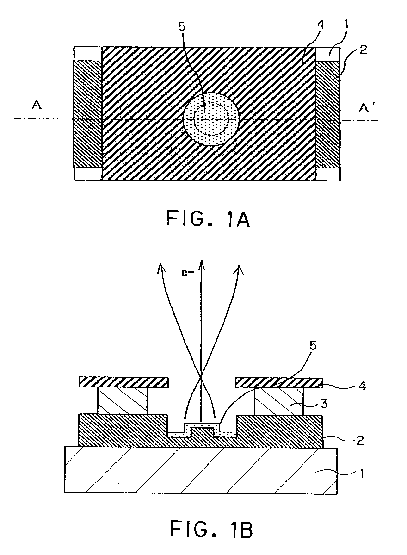
[0147] FIGS. 1A and 1B show Embodiment 1 of the present invention. Further, an example of a manufacturing method thereof is shown in FIGS. 4A to 4G. The manufacturing method is explained.
[0148] Process 1
[0149] First, soda lime glass is used as the substrate 1 as shown in FIG. 4A. Ta is formed to a thickness of 800 nm as the cathode electrode 2 after sufficient washing is performed.
[0150] Next, SiO.sub.2 is deposited to a thickness of 500 nm as the insulating layer 3, and Pt is deposited to a thickness of 100 nm as the gate electrode 4 in the stated order.
[0151] Process 2
[0152] In addition, the Al mask pattern 41 is formed as shown in FIG. 4B by utilizing photolithography.
[0153] Process 3
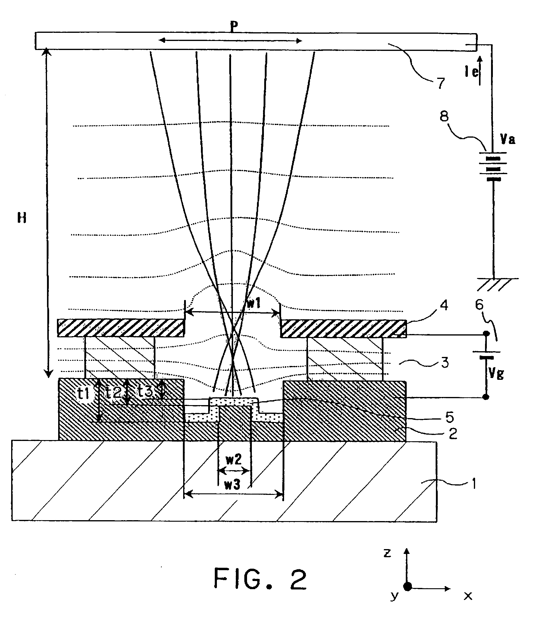
[0154] The Pt gate electrode 4 is then etched using Ar plasma etching, and the insulating layer 3 and the cathode electrode 2 are dry etched using CF.sub.4 gas, with the mask pattern 41 acting as a mask, as shown in FIG. 4C. An opening having the width w2 equal to 0.4 .mu.m, the width w3 equal to 1.2...
embodiment 2
[0167] FIG. 10A is a variation example of Embodiment 1, and is an example in which the edge is blunt in the process of manufacturing the cathode electrode 2.
[0168] The opening is minute in Embodiment 2, and for cases in which the peripheral portion region cannot be made small compared to the opening, the above-mentioned phenomenon is caused by etching. Manufacturing is performed in Embodiment 2 with the width w3 of the opening of the gate electrode 4 being set to 0.8 .mu.m.
[0169] A beam size similar to that of Embodiment 1 can also be obtained in Embodiment 2 by optimizing t3. In this case, it is also possible to manufacture the peripheral portion and the central portion of the opening bottom face of the cathode electrode 2 by also shaving the central portion of the cathode electrode 2 when manufacturing the peripheral portion, and performing the etching process, which must be performed twice in Embodiment 1, only once here.
embodiment 3
[0170] FIG. 10B is an example in which the size w1 of the opening of the gate electrode 4 is made smaller than the opening of the cathode electrode 2. In this structure, the electron-emitting material 5 does not exist in the edge portion of the cathode electrode 2, and therefore the leak current of the electron-emitting material 5 can be reduced to nearly zero.
[0171] A method of etching by using a focused ion beam from an oblique angle can be considered in etching the peripheral portion as a manufacturing method for forming this structure.
PUM
 Abstract
Description
Claims
Application Information