Time resolved non-invasive diagnostics system

Inactive Publication Date: 2003-05-29
DCG SYST
View PDF0 Cites 55 Cited by
  • Summary
  • Abstract
  • Description
  • Claims
  • Application Information

AI Technical Summary

Problems solved by technology

For example, avalanche breakdown in insulators cause light emission, and detection of such light emission can point to the locations of failure in the device.
Various emission microscopes have been used for detecting locations on the device where the electrical current drawn exceeds the expected levels and therefore could lead to locating failures in semiconductor devices.
One problem in probing flip chip packaged devices using conventional dynamic (timing) diagnostic methods, such as e-beam (voltage-contrast) probing, is that the critical nodes where timing information and fault isolation is critical are not readily accessible and masked by multiple levels of metal interconnects.
Th

Method used


Image

  • Time resolved non-invasive diagnostics system
  • Time resolved non-invasive diagnostics system
  • Time resolved non-invasive diagnostics system

Examples


Embodiment Construction

[0046] The present invention provides a testing system particularly suitable for rise time, timing; logic fault localization and other testing of microchips, especially from the backside through the substrate (e.g., flip chip packaged devices). Accordingly, the description proceeds with examples using flip chip. However, it should be appreciated that the invention is not limited to testing flip chips. For example, it is possible to take top-side packaged devices and "flip" them in a chip-scale package (CSP), or design the proper opening to ensure the emitted light gets through the top-side. What is desired is to be able to collect emission from a device of interest in the chip.

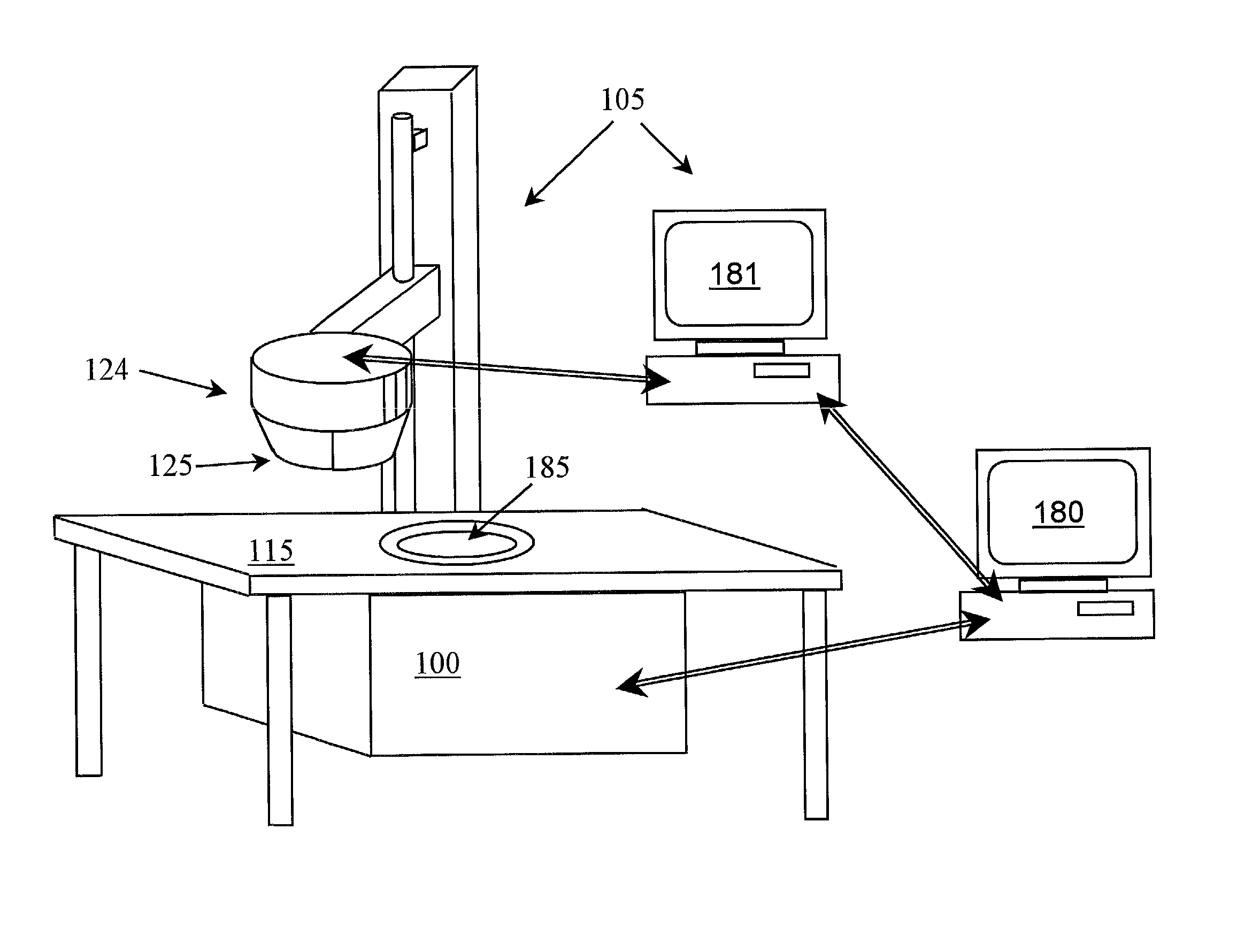
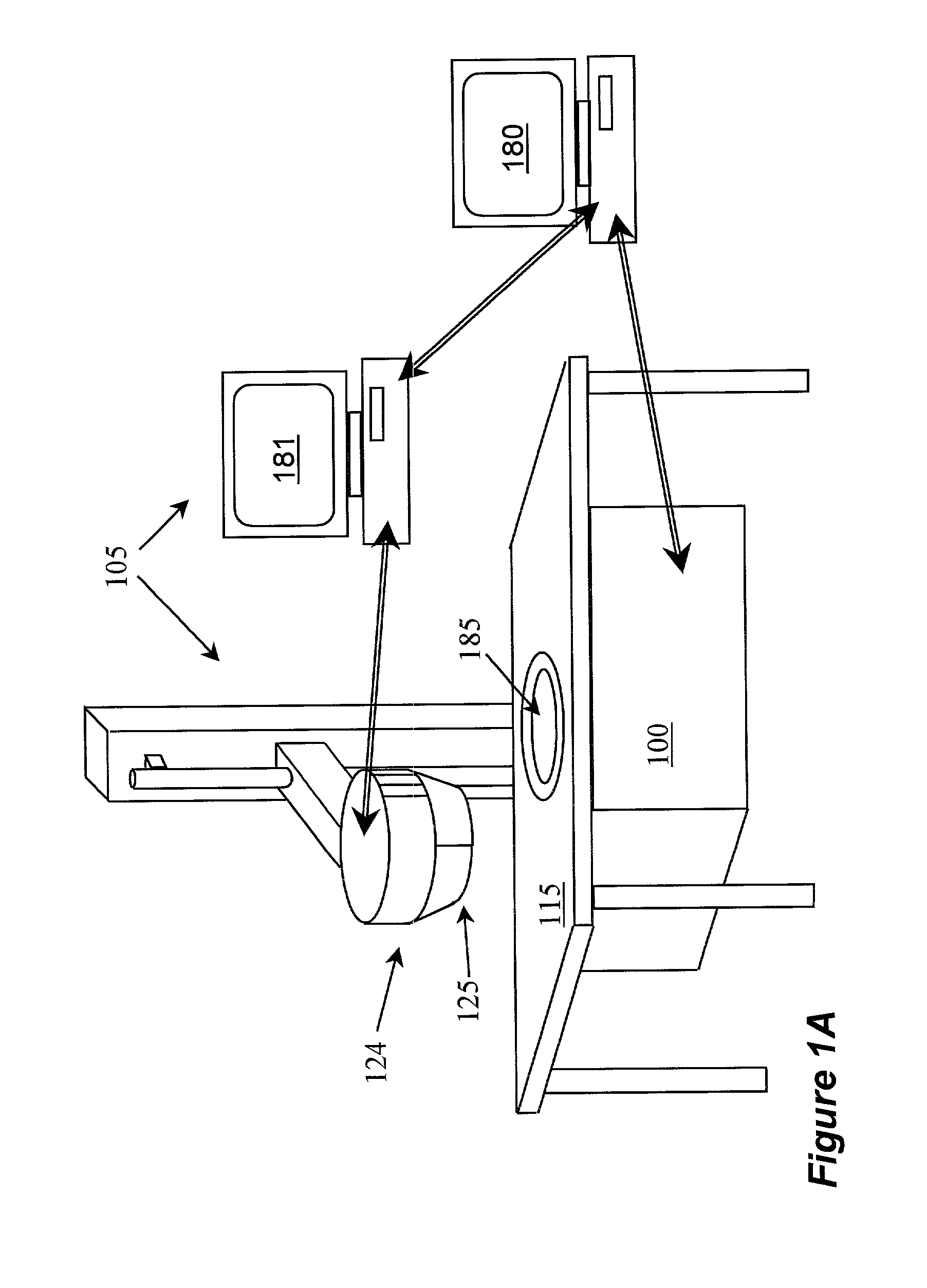
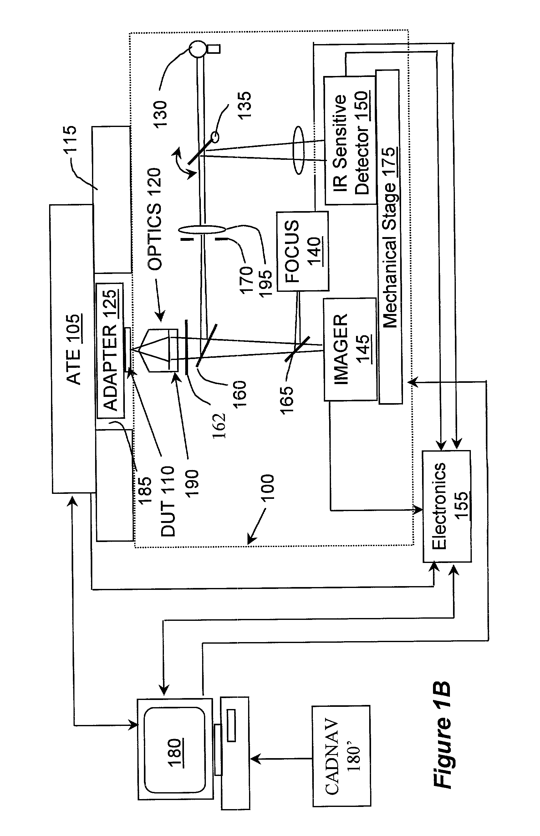
[0047] FIGS. 1A and 1B are general schematics depicting the major components of the testing and debug system according to an exemplary embodiment of the invention. The system operates in conjunction with a commercially available automated testing equipment 105 (ATE). The ATE generally comprises a controller, s...


PUM


Abstract

A system for probe-less non-invasive detection of electrical signals from integrated circuit devices is disclosed. The system includes an illumination source, collection optics, imaging optics, and a photon sensor. In a navigation mode, the light source is activated and the imaging optics is used to identify the target area on the chip and appropriately position the collection optics. Once the collection optics is appropriately positioned, the light source is deactivated and the photon sensor is used to detect photons emitted from the chip. No mention of cooling (active device measurement capability) and advanced optics to detect the features (SIL).

Description

[0001] 1. Field of the Invention[0002] The present invention relates to a system for in-situ transistor level measurement of circuit timing information directly related to the switching events (logic transitions) of switching events of transistors of electrically active semiconductor integrated circuits.[0003] 2. Description of the Related Art[0004] It is known in the prior art that various mechanisms in semiconductor devices can cause light emission. Detection of such light emission has been used to investigate semiconductor devices. For example, avalanche breakdown in insulators cause light emission, and detection of such light emission can point to the locations of failure in the device. Similar detection can be used to characterize electrostatic discharge in the device. In electrically stimulated (active) transistors accelerated carriers (electrons & holes), a.k.a. hot-carriers, emit light when the device draws current. Various emission microscopes have been used for detecting l...

Claims


Application Information

Patent Timeline
IPC IPC(8): G01R31/28G01R31/311
CPCG01R31/311G01N21/84
Inventor COTTON, DANIEL MURDOCHPAKDAMAN, NADERVICKERS, JAMES SQUIREWONG, THOMAS
Owner DCG SYST
Why Eureka
Try Eureka