Method of manufacturing optical waveguide and method of manufacturing OPTO-electric wiring board

a manufacturing method and technology of optical waveguide, applied in the field of manufacturing optical waveguide and manufacturing opto-electric wiring boards, can solve the problems of delaying electric signals, affecting the placement of other electronic devices, and affecting the performance of electronic devices, so as to reduce the time required and eliminate the stress remaining in the optical waveguide

Inactive Publication Date: 2003-07-10
NEC TOPPAN CIRCUIT SOLUTIONS
View PDF4 Cites 51 Cited by
  • Summary
  • Abstract
  • Description
  • Claims
  • Application Information

AI Technical Summary

Benefits of technology

[0026] It is therefore an object of the present invention to provide a method of manufacturing an optical waveguide, and a method of manufacturing an opto-electric wiring board which are capable of eliminating a stress remaining in the optical waveguide, and facilitating the handling of the optical waveguide during a manufacturing process to reduce a time required for manufacturing the opto-electric wiring board.
[0028] With the foregoing steps, the present invention eliminates any of the working step for stripping the optical waveguide resin layer from the first supporting substrate, the working step for adhering the stripped optical waveguide resin layer again to the second supporting substrate, the working step for stripping the optical waveguide resin layer from the second supporting substrate, and the like, otherwise required in the first prior art. Consequently, a shorter time is required for manufacturing the opto-electric wiring board to reduce the manufacturing cost. In addition, since the thin optical waveguide will not be left alone during the manufacturing, the optical waveguide is free from deformation, resulting in facilitated handling of the optical waveguide.
[0030] Since no stress remains in the photosensitive resin even if the optical waveguide is heated during the formation of the core layer, the resulting optical waveguide provides an improved reliability.

Problems solved by technology

Due to unwanted noise possibly generated during its operation, an electronic device adversely affects other electronic devices located nearby which would suffer from malfunctions, degraded performance, and the like.
Also, in the electronic device, electric signals may experience a delay associated with a time constant determined by capacitive and resistive components contained in electric wires.
If an optical waveguide is directly formed on the rugged surface for routing an optical line, the resulting optical waveguide will be distorted to cause a large transmission loss of an optical signal.
The first mentioned method of manufacturing an opto-electric wiring board according to the first prior art has a problem of a long manufacturing time and a resulting increase in cost due to the requirement of a plurality of types of supporting substrates which include first supporting substrate 101 for forming optical waveguide resin layer 103 that provides optical lines (optical waveguide), and second supporting substrate 105 for holding optical waveguide resin layer 103 stripped from first supporting substrate 101.
Thus, an additional time required for manufacturing the opto-electric wiring board causes an increase in the manufacturing cost.
Also, in the method of manufacturing an opto-electric wiring board according to the first prior art, thin optical waveguide resin layer 103 is susceptible to deformation into a curled layer when it is stripped from first supporting substrate 101, giving rise to a problem that optical waveguide resin layer 103 is hard to handle during the manufacturing process.
However, a long time is consumed for the adhesion particularly when optical waveguide resin layer 103 is reshaped into a flat layer with difficulties.
The method of manufacturing an optical waveguide according to the second prior art, on the other hand, has a problem of a residual stress produced in the optical waveguide because of the difference in thermal expansion coefficient between materials of the supporting substrate and optical waveguide.
The stress makes optical waveguide 118 more susceptible to cracking and the like, resulting in a lower long-term reliability of optical waveguide 118.

Method used


Image

  • Method of manufacturing optical waveguide and method of manufacturing OPTO-electric wiring board
  • Method of manufacturing optical waveguide and method of manufacturing OPTO-electric wiring board
  • Method of manufacturing optical waveguide and method of manufacturing OPTO-electric wiring board

Examples


first embodiment

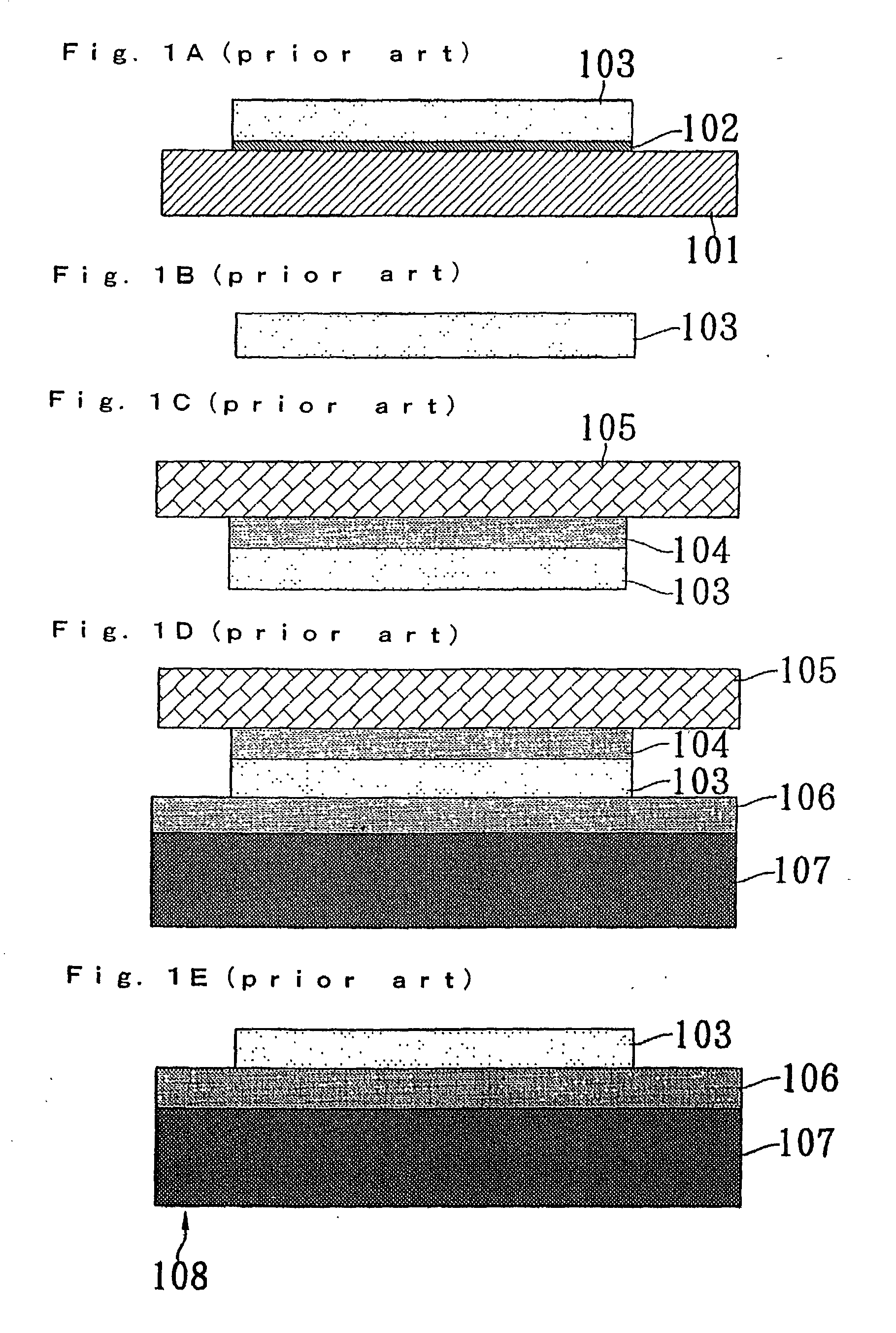
[0041] (First Embodiment)

[0042] FIGS. 3A to 3I are cross-sectional views illustrating a sequence of steps, one by one, in a first embodiment of a method of manufacturing an opto-electric wiring board according to the present invention. In the following, the method of manufacturing an opto-electric wiring board according to the first embodiment will be described with reference to FIGS. 3A to 3I.

[0043] In the first embodiment, a thermoplastic polycarbonate resin having a molecular weight in a range of 10,000 to 20,000 is used to form a supporting substrate 1 which is approximately 1 mm thick and in the shape of a square having one side of approximately 300 mm (see FIG. 3A). After an optical waveguide substrate including supporting substrate 1 is adhered to an electric wiring board, later described, supporting substrate 1 is dissolved using an organic solvent such as methylenechloride, tetrachloroethene, chloroform, 1,1,2-trichloroethane, chlorobenzene, dioxane, or the like.

[0044] When...

second embodiment

[0062] (Second Embodiment)

[0063] FIGS. 4A to 4F are cross-sectional views illustrating a sequence of steps, one by one, in a second embodiment of a method of manufacturing an opto-electric wiring board according to the present invention.

[0064] The method of manufacturing an opto-electric wiring board according to the second embodiment differs from the first embodiment in that the former employs a supporting substrate which has a higher heat distortion temperature.

[0065] In the following, the method of manufacturing an opto-electric wiring board according to the second embodiment will be described with reference to FIGS. 4A to 4F.

[0066] In the second embodiment, a thermoplastic polyphenylene sulfide (PPS) resin is used to form supporting substrate 11 which is approximately 1 mm thick and in the shape of a square having one side of approximately 300 mm (see FIG. 4A). The PPS resin is a crystalline polymer which exhibits a heat distortion temperature of approximately 260.degree. C. nea...

third embodiment

[0083] (Third Embodiment)

[0084] FIGS. 5A to 5H are cross-sectional views illustrating a sequence of steps, one by one, in a third embodiment of a method of manufacturing an opto-electric wiring board according to the present invention.

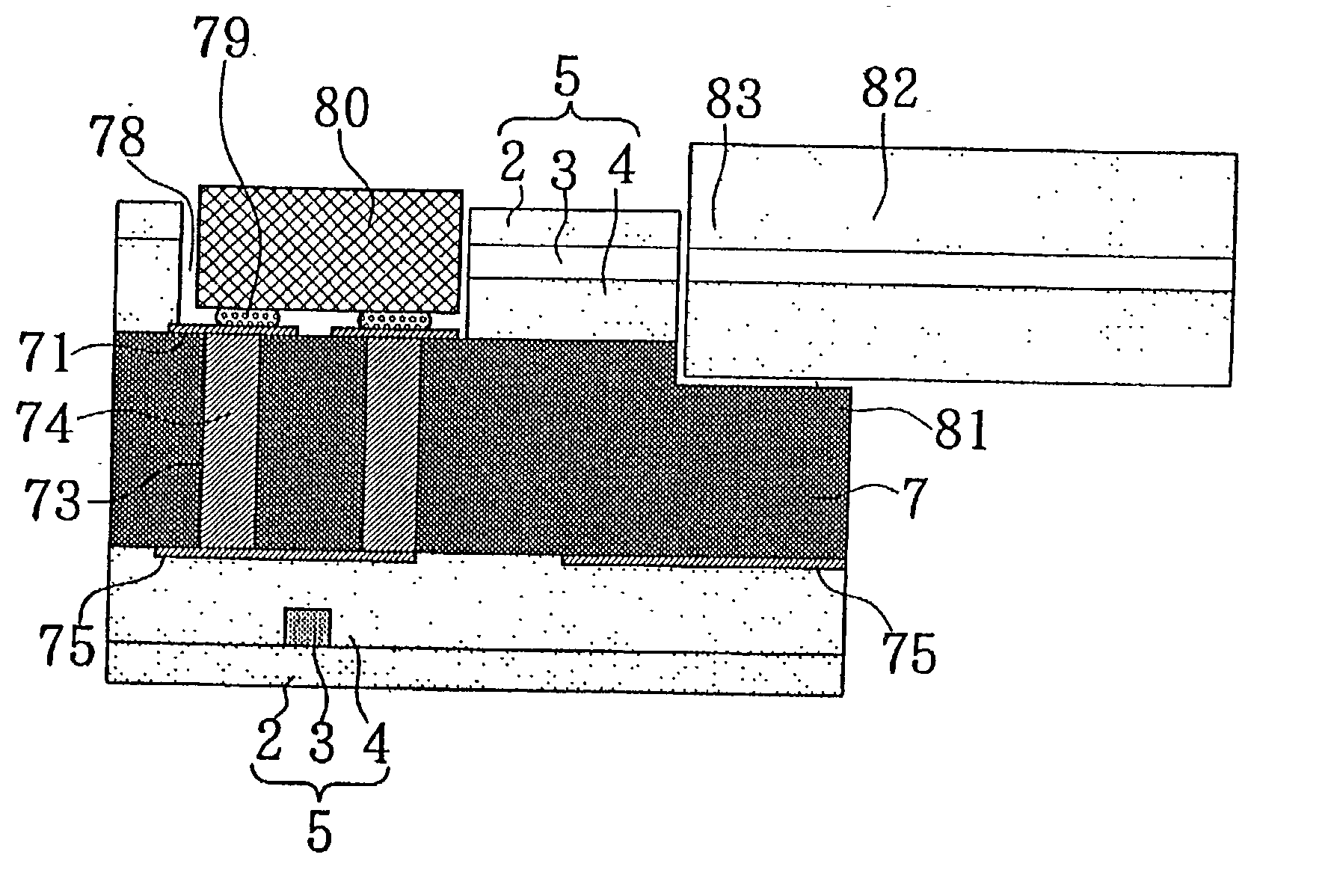
[0085] The method of manufacturing an opto-electric wiring board according to the third embodiment differs from the first embodiment in that electric wires routed on the opto-electric wiring board have a certain degree of freedom.

[0086] In the following, the method of manufacturing an opto-electric wiring board according to the third embodiment will be described with reference to FIGS. 5A to 5H.

[0087] In the third embodiment, first, optical waveguide 25 having core layer 23 between lower cladding layer 22 and upper cladding layer 24 is formed on supporting substrate 21 through steps similar to those in the first embodiment illustrated in FIGS. 3A to 3D to complete optical waveguide substrate 26 illustrated in FIG. 5A. This optical waveguide substrate 2...


PUM


Abstract

After an optical waveguide substrate including a supporting substrate is adhered to an electric wiring board, the supporting substrate alone is dissolved using an organic solvent for removal. Alternatively, the supporting substrate alone is melted through a thermal treatment for removal. Further, a core layer of an optical waveguide is formed on the substrate using a photosensitive resin having a thermal expansion coefficient substantially identical to that of the supporting substrate.

Description

BACKGROUND OF THE INVENTION[0001] 1. Field of the Invention[0002] The present invention relates to a method of manufacturing an optical waveguide for use as an optical line, and a method of manufacturing an opto-electric wiring board which comprises optical waveguides and electric wires mixedly formed thereon.[0003] 2. Description of the Related Art[0004] Generally, electronic parts such as LSI (Large Scale Integrated Circuit) are mounted on electric wiring boards formed with electric wires for assembly into a variety of electronic devices. An electronic device implements a predetermined function by transmitting electric signals through electric wires which interconnect respective electronic parts. Due to unwanted noise possibly generated during its operation, an electronic device adversely affects other electronic devices located nearby which would suffer from malfunctions, degraded performance, and the like. Also, in the electronic device, electric signals may experience a delay a...

Claims


Application Information

Patent Timeline
Patent Type & Authority Applications(United States)
IPC IPC(8): G02B6/12G02B6/42G02B6/13G02B6/43H05K1/02H05K3/00
CPCG02B6/138G02B6/305G02B6/42G02B6/4202G02B6/4204H05K1/0274G02B6/423G02B6/43G02B2006/12069G02B2006/1215G02B2006/12159G02B6/4228
Inventor KIKUCHI, HIDEOODA, MIKIOKOUTA, HIKARUKITAJO, SAKAESHIMADA, YUZO
Owner NEC TOPPAN CIRCUIT SOLUTIONS
Why Eureka
Try Eureka