CMP slurry additive for foreign matter detection

a technology of foreign matter and additive, which is applied in the direction of manufacturing tools, cleaning with liquids, lapping machines, etc., can solve the problems of severe foreign matter problems and defects, high defect level observed on post-cmp cleaned wafers, and create electrical short defects

Inactive Publication Date: 2003-07-24
IBM CORP
View PDF9 Cites 22 Cited by
  • Summary
  • Abstract
  • Description
  • Claims
  • Application Information

AI Technical Summary

Problems solved by technology

One of the major disadvantages of CMP is the higher defect level observed on post-CMP cleaned wafers.
Slurry residue often becomes detached from wafers during subsequent processing, causing severe foreign matter (FM) problems and defects.
For example, if the slurry is buried inside metal during sputtering, it will create an electrical short defect after subsequent patterning b...

Method used


Image

  • CMP slurry additive for foreign matter detection
  • CMP slurry additive for foreign matter detection
  • CMP slurry additive for foreign matter detection

Examples


Embodiment Construction

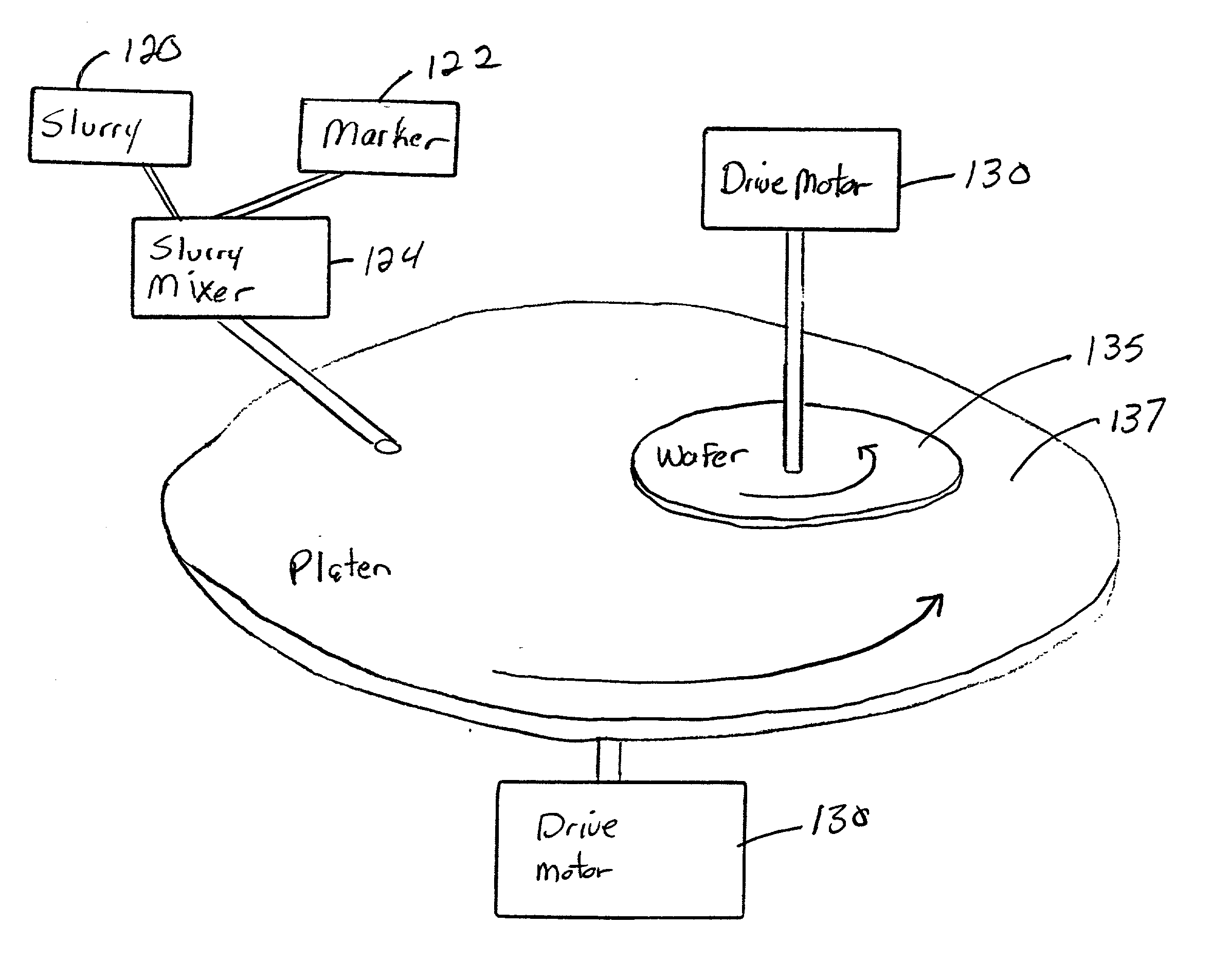
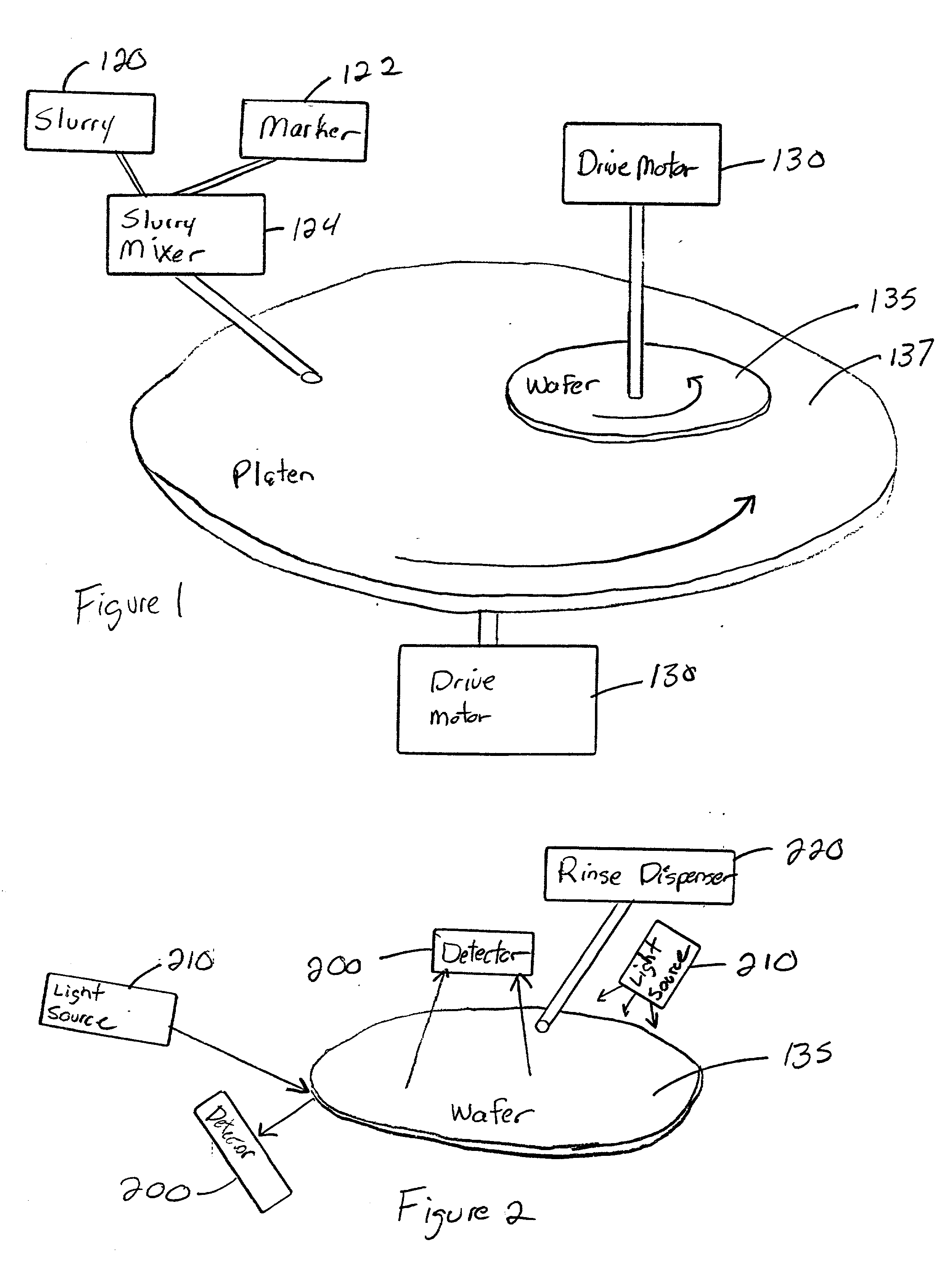
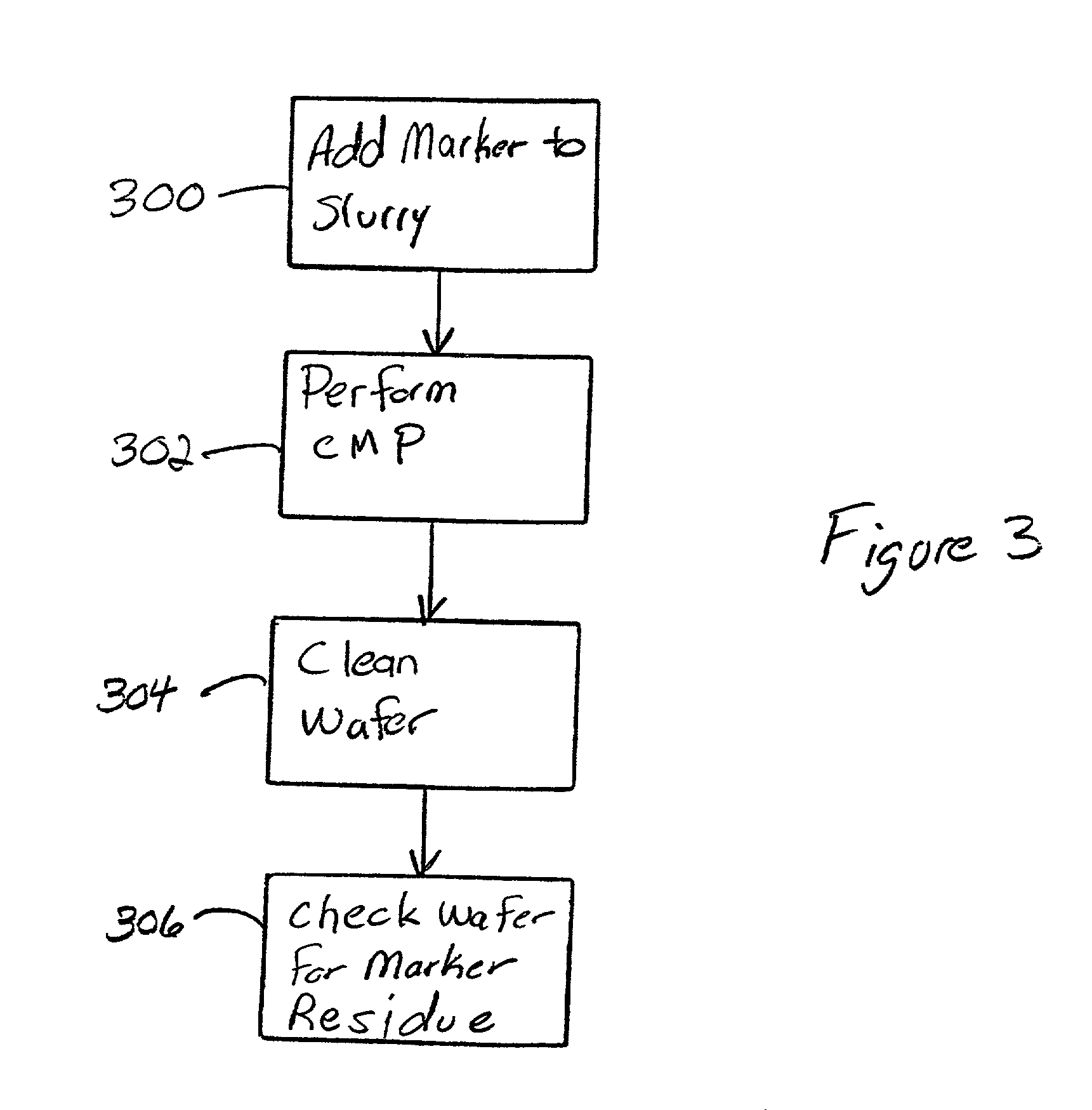
[0016] In order to overcome the conventional problems of detecting slurry residue on silicon wafers that are discussed above, the invention adds a marker to the slurry. The marker is added in a very small quantity so that it will not affect the polishing characteristic of the regular slurry. An example of an acceptable percentage range that the marker would make up of the slurry mixture is fluorescence or phosphorescence dye in the 1 to 100 ppm range and volatile organics additives in the 10 to 500 ppm range.

[0017] For example, as shown in FIG. 1, the invention includes a marker container 122 from which marker material is mixed with slurry from a slurry container 120 in a slurry mixture container 124. The slurry mixture container 124 supplies the slurry mixture to the platen 137 which is rotated by a drive motor 130. The silicon wafer 135 is also rotated by drive motor 130 and moves around the rotating platen 137. This action polishes the side of the wafer 135 that is in contact wit...


PUM

PropertyMeasurementUnit
Pressureaaaaaaaaaa
Fluorescenceaaaaaaaaaa
Vapor pressureaaaaaaaaaa

Abstract

A method and structure polishes and cleans silicon wafers by mixing a marker with a slurry to form a slurry mixture, performs chemical mechanical polishing on a silicon wafer using the slurry mixture, rinses the slurry mixture from the silicon wafer, checks the silicon wafer for marker residue, and repeats the rinsing process if the checking process detects the marker residue on the wafer.

Description

[0001] 1. Field of the Invention[0002] The present invention generally relates to chemical mechanical polishing (CMP) processes and more particularly to an improved process that utilizes a marker with the slurry mixture that more clearly indicates whether the slurry has been completely rinsed from the silicon wafer after the CMP process has been completed.[0003] 2. Description of the Related Art[0004] In the manufacture of integrated circuits, semiconductor wafer surface planarity is of extreme importance. To achieve the degree of planarity required to produce ultra high density integrated circuits, chemical-mechanical polishing / planarization (CMP) is often employed. The terms "planarization" and "polishing" as used herein are interchangeable when referring to the technique of "CMP." In general, CMP involves holding a semiconductor wafer against a moving polishing surface that is wetted with a chemically reactive, abrasive material or slurry, such as silica or alumina. For example, ...

Claims


Application Information

Patent Timeline
IPC IPC(8): B08B3/00B08B3/02B24B37/04H01L21/306
CPCB08B3/00B08B3/02H01L21/02052H01L21/02024B24B37/042
Inventor WONG, KWONG HONBOGGS, KARL E.MITCHELL, RAPHAELZIEMINS, ULDIS A.
Owner IBM CORP
Why Eureka
Try Eureka