Semiconductor device, nonvolatile semiconductor storage apparatus using the device, and manufacture method of the device

a semiconductor storage and semiconductor technology, applied in semiconductor devices, transistors, instruments, etc., can solve the problems of large burden on the charge pumping circuit, difficult to establish high integration and low power consumption, and limited number of cells to be written at the same time, so as to enhance the insulating property between the first floating gate and the isolating gate, and improve the reliability during application of high voltage. , the effect of enhancing the insulating property

Inactive Publication Date: 2003-07-31
RENESAS ELECTRONICS CORP
View PDF2 Cites 14 Cited by
  • Summary
  • Abstract
  • Description
  • Claims
  • Application Information

AI Technical Summary

Benefits of technology

[0025] Moreover, by forming an isolating gate parallel to the first floating gate with an isolating insulating film therebetween, an element isolation function during application of the high voltage is secured, leak current or the like fails to easily occur, and as a result, incorrect operation is eliminated and reliability is enhanced.
[0037] In the manufacture method of the semiconductor device, by using a conventional manufacture apparatus as it is, and only slightly clanging a manufacture process, the semiconductor device can easily be manufactured in which the isolating gate is formed on the second floating gate on the side of the semiconductor substrate, and parallel to the first floating gate via the isolating insulating film.

Problems solved by technology

However, it is very difficult to establish both high integration and low power consumption as described later.
Therefore, a burden to the charge pumping circuit is large, and the number of cells to be written at the same time is limited, or a chip size is enlarged since capacitors of the charge pumping circuit must be large.
Alternatively, another phenomenon disadvantageously occurs in which the writing inhibition voltage also exerts an influence on the adjacent cell and the writing is not performed.
However, since the isolation structure itself is large, memory cell size is increased, and it is disadvantageously difficult to raise an integration degree.
As a result, a large coupling capacity ratio R.sub.c cannot be secured, and it is disadvantageously difficult to realize a low voltage.

Method used


Image

  • Semiconductor device, nonvolatile semiconductor storage apparatus using the device, and manufacture method of the device
  • Semiconductor device, nonvolatile semiconductor storage apparatus using the device, and manufacture method of the device
  • Semiconductor device, nonvolatile semiconductor storage apparatus using the device, and manufacture method of the device

Examples


Embodiment Construction

[0062] A semiconductor device, nonvolatile semiconductor storage apparatus using the device and manufacture method according to one embodiment of the present invention will be described with reference to the drawings. It is understood that the invention is not limited to this embodiment, which is provided as only one example of an implementation of the invention. For example the invention is not restricted to EEPROMS, is applicable to other memories such as flash memories and memories in general where the memory cell isolation is a concern

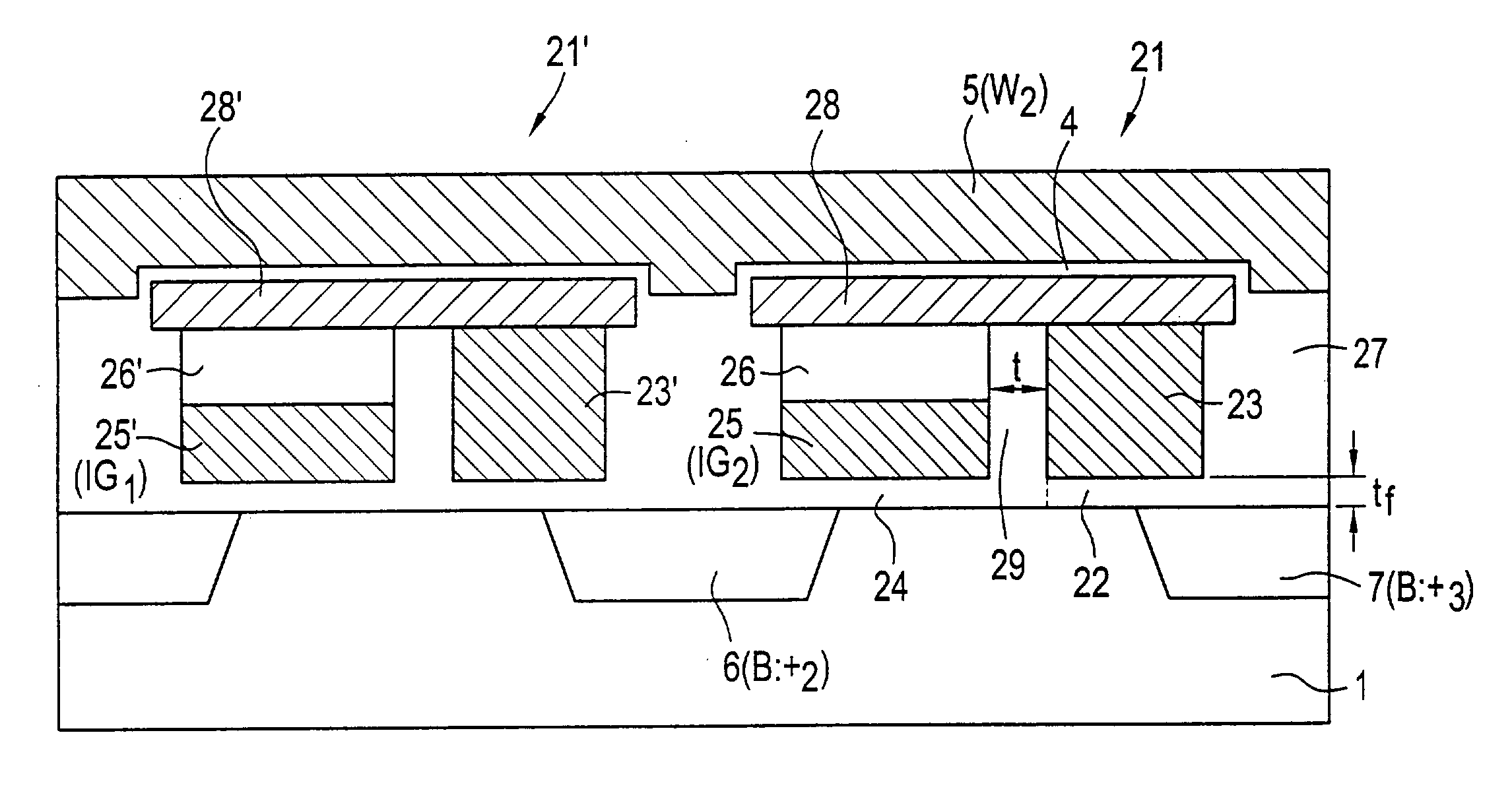
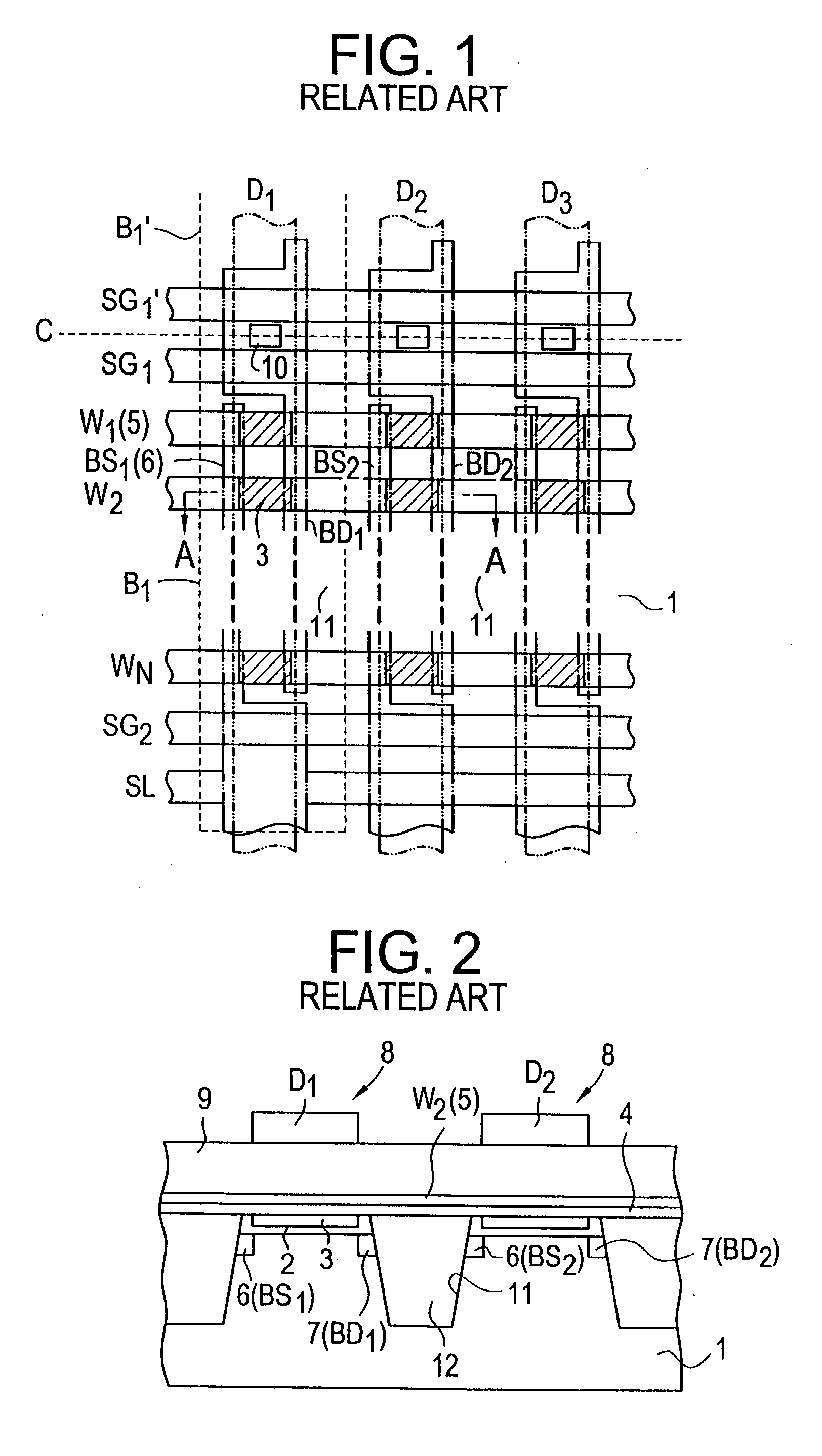
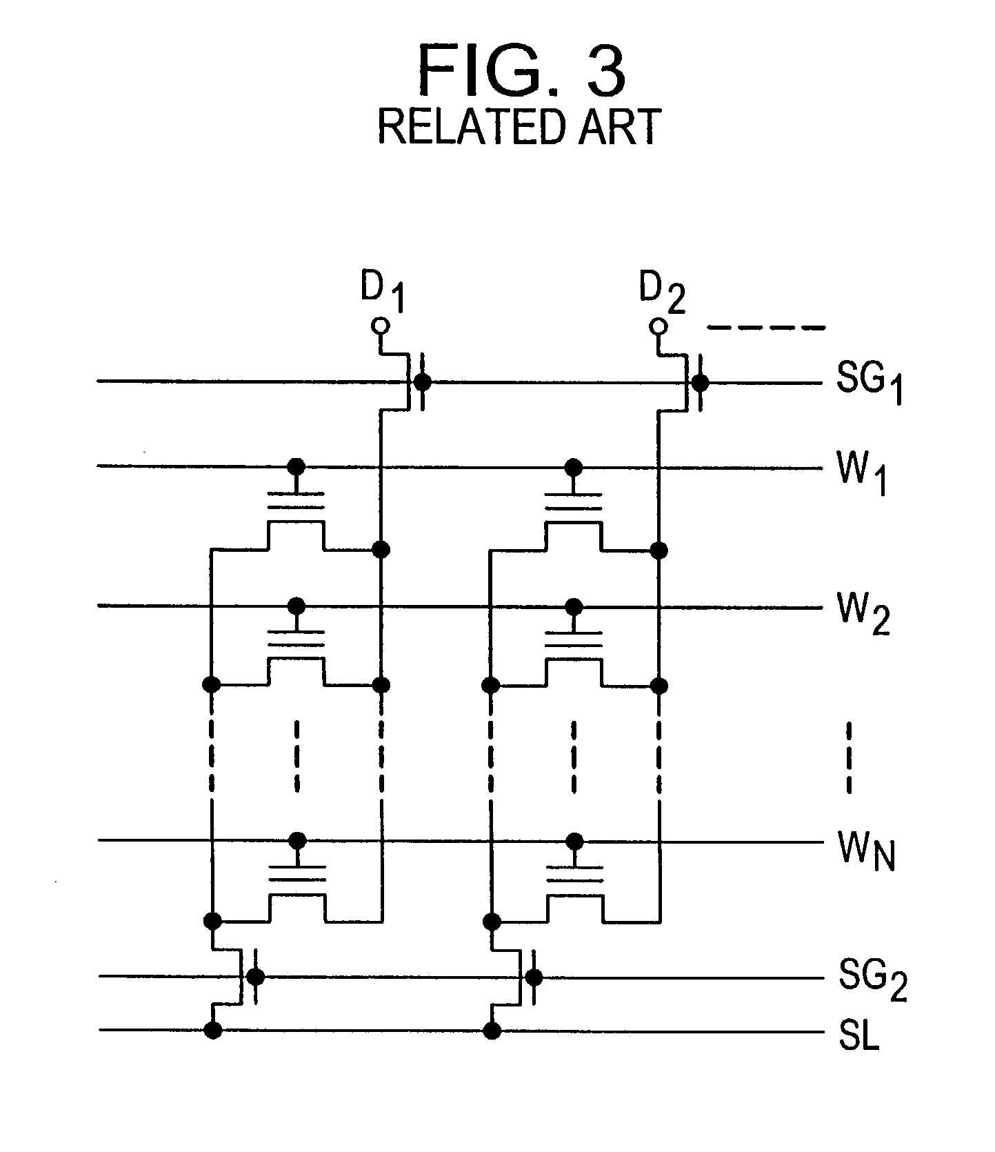
[0063] FIG. 4 is a plan view showing a main part of a memory array Of all EEPROM which is an example of a nonvolatile semiconductor storage apparatus that may advantageously use the present invention, FIG. 5 is an equivalent circuit of the memory array of FIG. 4, and FIG. 6 is a sectional view along line B-B of FIG. 4.

[0064] Referring to FIGS. 4-6, the main surface of a memory array area of a p-type silicon substrate (semiconductor substrate) 1 is ...


PUM


Abstract

[Problem] There are provided a semiconductor device which is operable with a small occupied area, high reliability, and low power consumption, a nonvolatile semiconductor storage apparatus using the device and a manufacture method of the device. [Solution Means] A semiconductor device of the present invention comprises a first gate insulating film 22, floating gate, second gate insulating film 4, and control gate 5 on a semiconductor substrate 1, and a source area 6 and a drain area 7 formed in the semiconductor substrate 1 on opposite sides of the floating gate, the floating gate comprises a first floating gate 23 and a second floating gate 28 disposed to cover the first floating gate 23, and an isolating gate 25 is formed on the second floating gate 28 on the side of the semiconductor substrate 1, and parallel to the first floating gate 23 via an isolating insulating film 26.

Description

[0001] 1. Field of the Invention[0002] The present invention relates to a semiconductor device, a nonvolatile semiconductor storage apparatus using the device and a manufacture method of the device, particularly but not limited to a preferable semiconductor device for use in an electrically erasable and programmable read only memory (EEPROM), and the like, a nonvolatile semiconductor storage apparatus using the device and a manufacture method of the device.[0003] 2. Description of the Related Art[0004] One type of a conventional nonvolatile semiconductor memory (which is mainly ROM) are various EEPROMs. In such a memory frequently perform data writing, erasing, reading, and the like are performed electrically, and rewritten data is held for a very long time.[0005] In the EEPROM, a cell structure is of a two-layer gate type in which, for example, a floating gate is formed on a transistor channel area via a first gate insulating film, and a control gate is formed on the floating gate ...

Claims


Application Information

Patent Timeline
Patent Type & Authority Applications(United States)
IPC IPC(8): G11C16/04H01L21/8247H01L27/115H01L29/423H01L29/788H01L29/792
CPCG11C16/0433H01L27/115H01L29/7883H01L29/42324H01L29/42328H01L27/11521H10B69/00H10B41/30
Inventor HAYASHI, FUMIHIKO
Owner RENESAS ELECTRONICS CORP
Why Eureka
Try Eureka