Light modulating device

a technology of light modulating device and light source, which is applied in the direction of identification means, instruments, optics, etc., can solve the problems of large substrate, difficult to set appropriate driving conditions with such a high resolution, and difficulty in producing color liquid crystal panels with a resolution of 600 dpi or mor

Inactive Publication Date: 2003-10-02
SHARP KK
View PDF3 Cites 53 Cited by
  • Summary
  • Abstract
  • Description
  • Claims
  • Application Information

AI Technical Summary

Problems solved by technology

However, it is very difficult to produce a color liquid crystal panel having a resolution of 600 dpi or more with production apparatuses that are commonly used in the art.
In addition, as to the driving circuit, it is difficult to set appropriate driving conditions with such a high resolution.
With large-size LCDs, however, the substrate is also large, whereby the realization of large-size high-resolution LCDs is hindered by problems such as a delay in the voltage application at locations remote from the signal-input side.
However, with the liquid crystal display device disclosed in Japanese Laid-Open Patent Publication No. 2000-284315, the light scattering effect is dependent on the thickness of the polymer-dispersed liquid crystal layer, and the thickness of the polymer-dispersed liquid crystal layer needs to be quite large to obtain a scattering effect that is strong enough to convert RGB light into white light, thereby requiring a very large voltage to be applied.
Moreover, since the transmittance cannot be controlled to an intended value, it is highly likely that an intended hue is not obtained in a color display.
Furthermore, since two panels are layered together, a color shift may occur across the displayed image in a color display, and the display may appear in an incongruent manner because of a transmittance shift across a picture element in a monochrome display, due to the parallax between the monochrome liquid crystal panel and the ECB liquid crystal panel.

Method used


Image

  • Light modulating device
  • Light modulating device
  • Light modulating device

Examples


Embodiment Construction

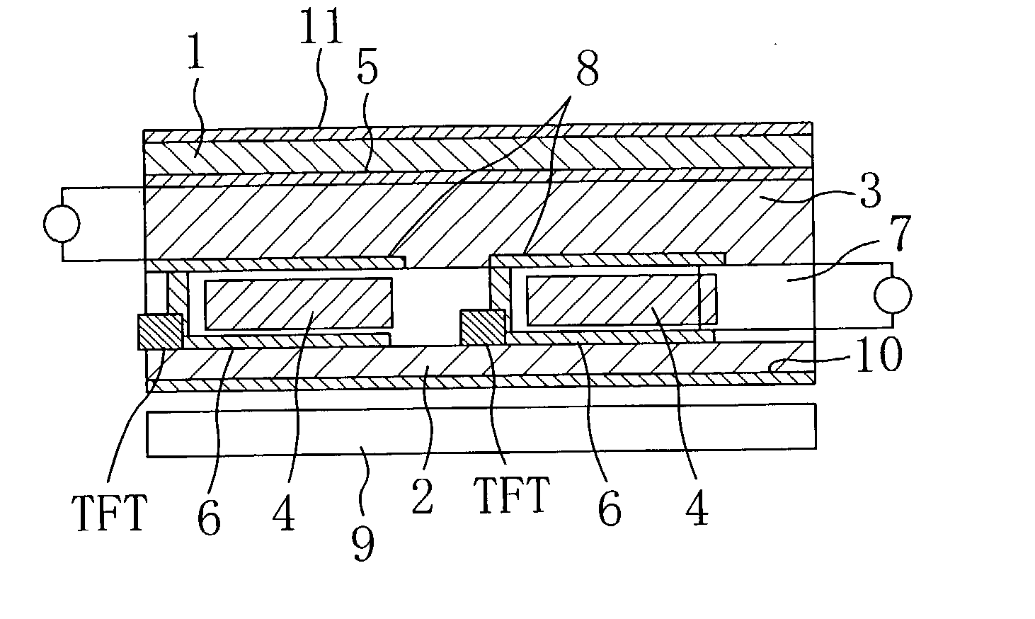
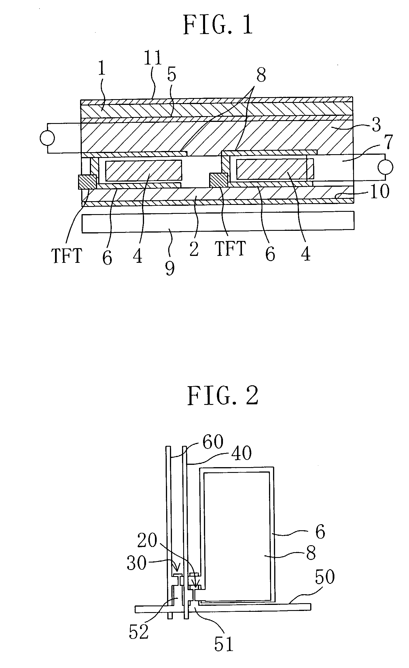
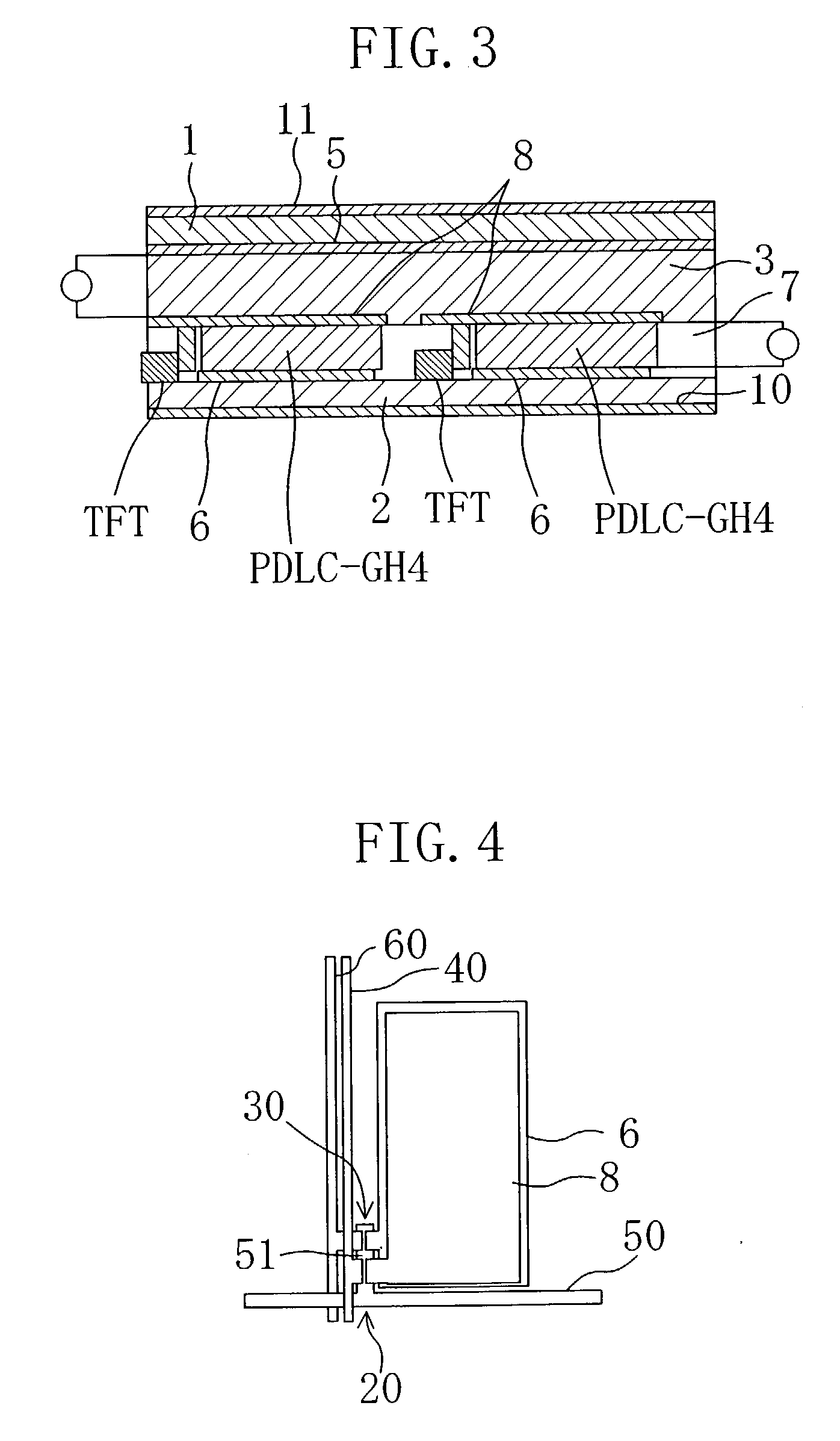
[0082] FIG. 7 is a cross-sectional view schematically illustrating a light modulating device of a comparative example, shown in comparison with the light modulating device of the present invention. The light modulating device of the comparative example includes two panels, i.e., a color filter panel 100 and a liquid crystal panel 110. A color filter layer whose colored / uncolored state is electrically controlled is formed on the color filter panel 100. In other words, the color filter layer and the liquid crystal layer are each interposed between a pair of substrates and a pair of electrode layers.

[0083] When an image is displayed on the screen while some of the color filter layers are uncolored by being switched by the color filter panel 100, the high-resolution monochrome / color divided display can be observed from a direction normal to the screen. However, when the light modulating device of the comparative example is observed from a slightly-inclined viewing angle, a color shift o...


PUM

PropertyMeasurementUnit
peak wavelengthaaaaaaaaaa
organic electrochromicaaaaaaaaaa
electroluminescenceaaaaaaaaaa

Abstract

A light modulating device includes: a first substrate on which a first electrode layer and a light amount control layer are deposited in this order; a second substrate on which a second electrode layer and a color filter layer are deposited in this order, the second substrate opposing the first substrate; and a third electrode layer interposed between the light amount control layer and the color filter layer, wherein a plurality of picture elements are defined in a matrix pattern by the first electrode layer and the third electrode layer. An amount of light transmitted through the light amount control layer is electrically controlled by the first electrode layer and the third electrode layer. A colored/uncolored state of the color filter layer is electrically controlled by the second electrode layer and the third electrode layer.

Description

[0001] 1. Field of the Invention[0002] The present invention relates to a light modulating device, and more particularly to a light modulating device capable of producing a color display and a high-resolution monochrome display. The light modulating device of the present invention may be used in a transmission type liquid crystal display device, a reflection type liquid crystal display device, a transmission / reflection type liquid crystal display device, an organic or inorganic EL (electroluminescence) device, an electrophoretic device, and an image reading device.[0003] 2. Description of the Background Art[0004] Liquid crystal displays (LCDs) have been used in various applications, primarily in personal applications, for their advantageous features such as a small installation space and a small power consumption. It is expected that LCDs will be used in a wider range of applications and under more various circumstances. An LCD is provided with a color filter for producing a color d...

Claims


Application Information

Patent Timeline
Patent Type & Authority Applications(United States)
IPC IPC(8): G02B5/20G02F1/1334G02F1/1335G02F1/1347G02F1/1516G09F9/30G09F9/35
CPCG02F1/1334G02F1/133514G02F2201/44G02F1/15G02F1/13475G02F1/1516
Inventor NAGAE, NOBUKAZU
Owner SHARP KK
Why Eureka
Try Eureka