

Atomic layer deposition of tungsten barrier layers using tungsten carbonyls and boranes for copper metallization
- Summary
- Abstract
- Description
- Claims
- Application Information
AI Technical Summary
Problems solved by technology
Method used
Image

Examples
Embodiment Construction
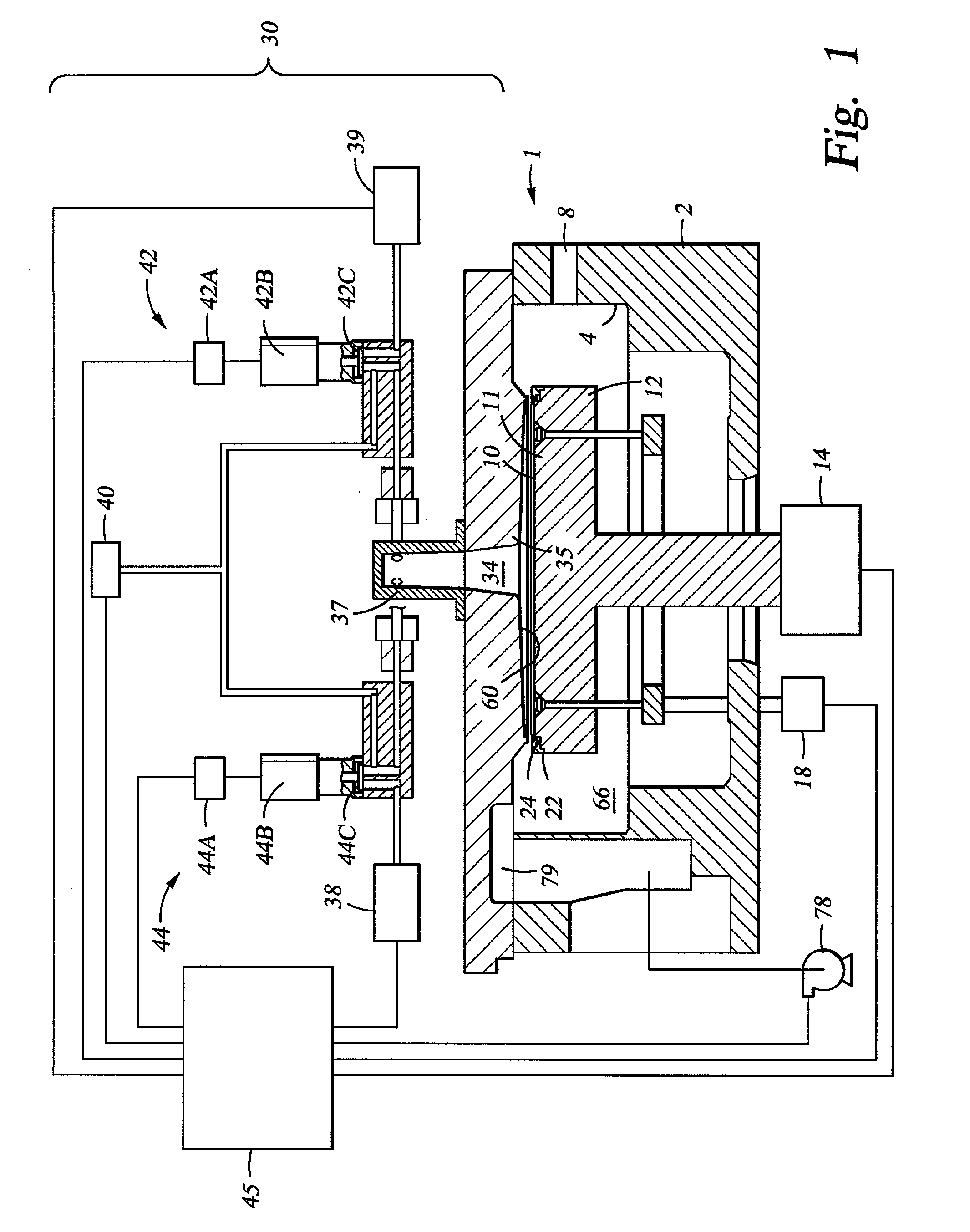
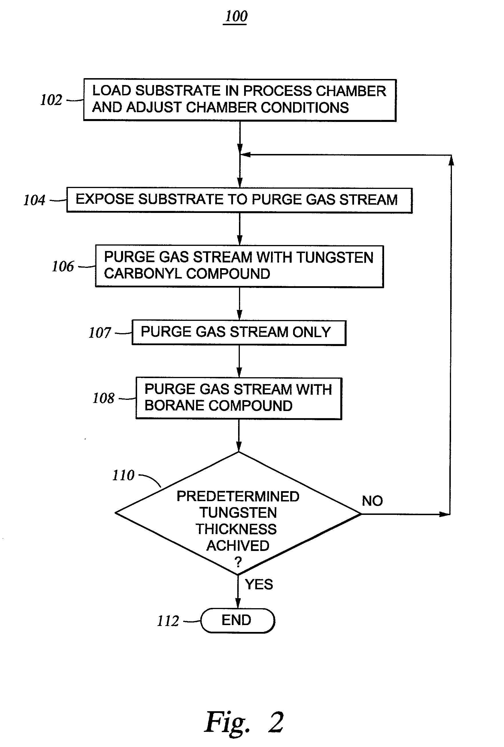
[0046] A tungsten layer having excellent barrier properties and excellent adhesion to dielectric layers is deposited in the chamber of FIG. 1 with a heater temperature of 250.degree. C. at 0.7 torr by flowing tungsten hexacarbonyl at 15 sccm and argon at 250 sccm for 0.5 seconds, flowing argon alone at 1000 sccm for 1 second, flowing diborane at 25 sccm and argon at 500 sccm for 1 second, and then flowing argon alone at 1000 sccm for 1 second. Repetition of these steps for 30 cycles deposits a tungsten layer having a thickness of about 30 .ANG..
[0047] Copper Metallization
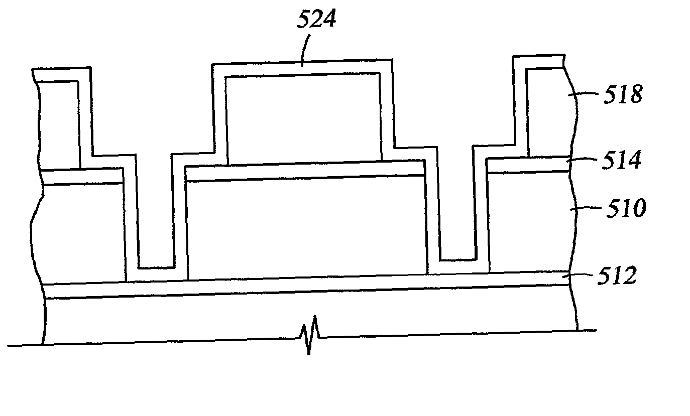
[0048] As shown in FIG. 4A, a first dielectric layer 510, such as parylene, silicon oxide, fluorine doped silicon oxide (e.g., FSG), spin on glass, carbon doped silicon oxide (e.g., Black Diamond.TM. silicon oxide available from Applied Materials, Inc.), SiLK.TM. silicon oxide, or the like, is deposited on a substrate 512. The thickness of the first dielectric layer 510 and subsequent layers described below will var...
PUM
| Property | Measurement | Unit |
|---|---|---|
| Flow rate | aaaaa | aaaaa |
| Adhesion strength | aaaaa | aaaaa |
| Semiconductor properties | aaaaa | aaaaa |
Abstract
Description
Claims
Application Information