Methods, systems, and apparatus for atomic-layer deposition of aluminum oxides in integrated circuits

a technology of integrated circuits and aluminum oxides, applied in the direction of pretreatment surfaces, coatings, metal material coating processes, etc., can solve the problems of non-uniform thickness, difficult, if not impossible, for cvd to provide uniform coverage of trench sidewalls

Inactive Publication Date: 2003-11-06
MICRON TECH INC
View PDF99 Cites 501 Cited by
  • Summary
  • Abstract
  • Description
  • Claims
  • Application Information

AI Technical Summary

Problems solved by technology

Conventional chemical-vapor-deposition (CVD) systems suffer from at least two problems.
First, conventional CVD systems generally form non-uniformly thick layers that include microscopic hills and valleys, and thus generally require use of post-deposition planarization or other compensation techniques.
Second, it is difficult, if not impossible, for CVD to provide uniform coverage of trench sidewalls or complete filling of holes and trenches.
However, the present inventors have recognized that the equipment and processes reported as optimal for thin-film head applications suffer from some limitations relative to use in fabricating integrated circuits.
Moreover, the reported equipment uses a larger than desirable reaction chamber, which takes longer to fill up or pump out, and thus prolongs the duration of each deposition cycle.

Method used


Image

  • Methods, systems, and apparatus for atomic-layer deposition of aluminum oxides in integrated circuits
  • Methods, systems, and apparatus for atomic-layer deposition of aluminum oxides in integrated circuits
  • Methods, systems, and apparatus for atomic-layer deposition of aluminum oxides in integrated circuits

Examples


Embodiment Construction

)

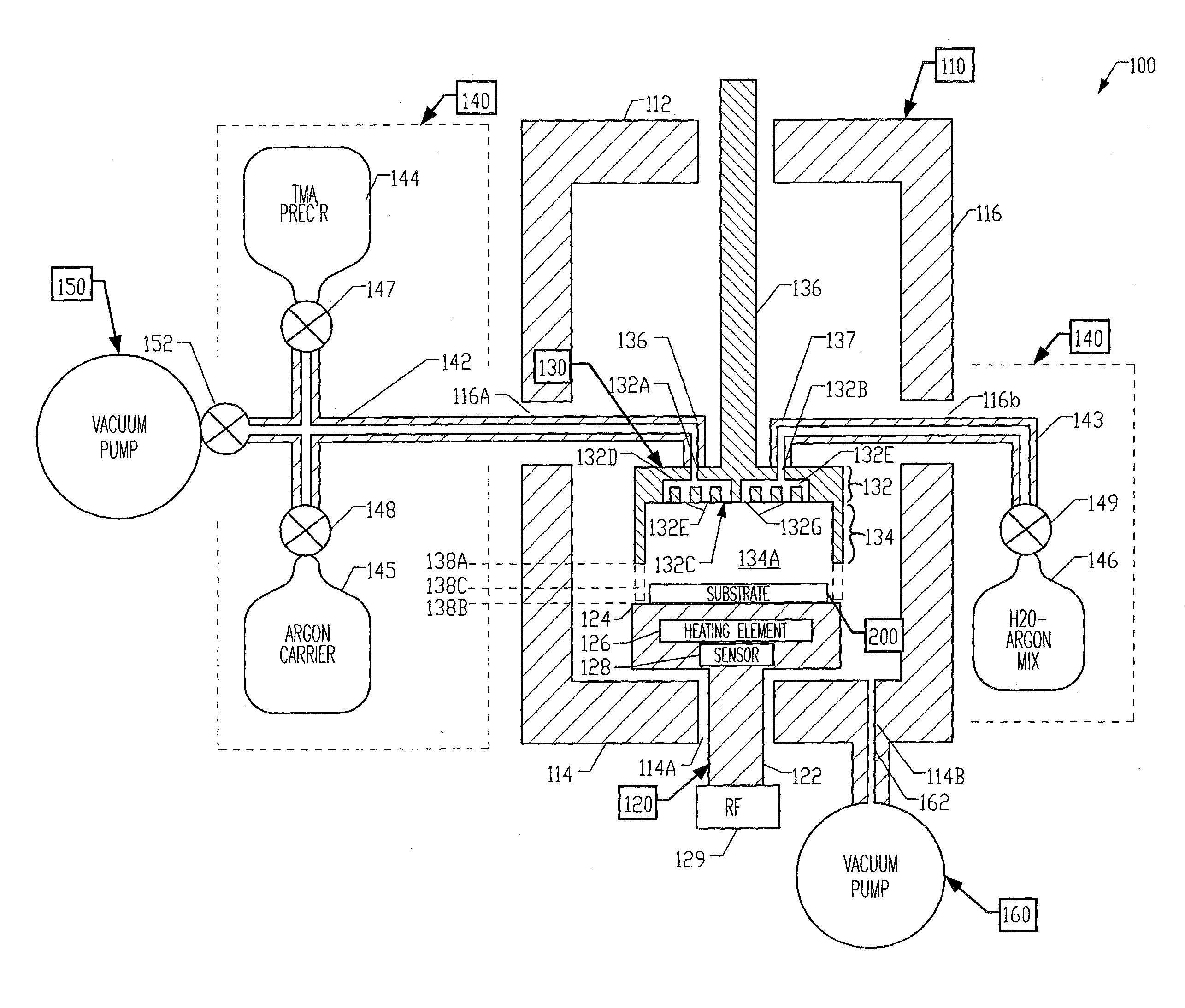
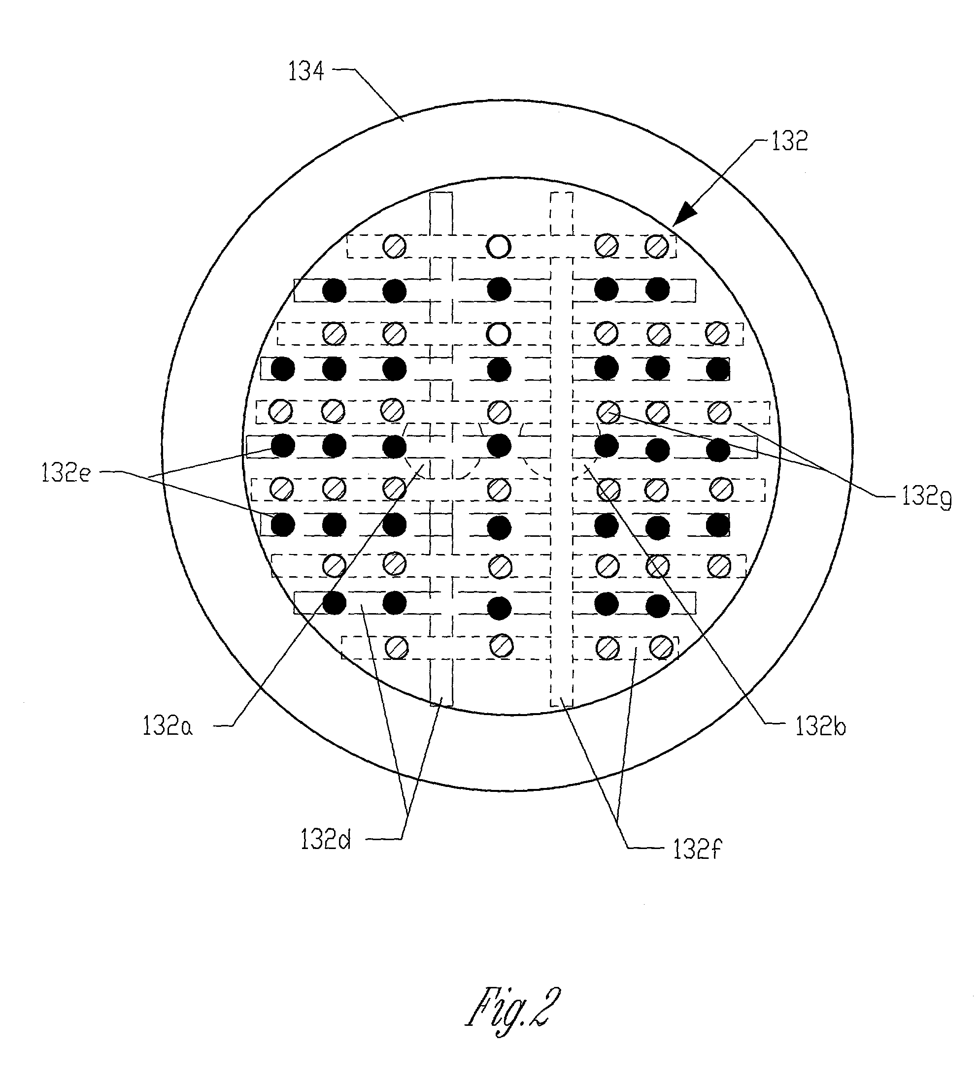
[0009] To address these and / or other problems, the present inventor devised new systems, methods, and apparatuses for atomic layer deposition. One exemplary atomic-layer deposition system, well suited for aluminum-oxide depositions in integrated-circuit fabrication, includes an outer chamber, a substrate holder, and a unique gas-distribution fixture. The fixture includes a gas-distribution surface having two sets of holes and a gas-confinement member that forms a wall around the holes. In operation, one set of holes dispenses an aluminum-carrying precursor and the other dispensing an oxidizing agent gas, after the gas-confinement member engages, or otherwise cooperates with the substrate holder to form an inner chamber within the outer chamber.

[0010] The inner chamber has a smaller volume than the outer chamber and thus consumes less gas during the deposition process than would the outer chamber used alone. Also, the smaller chamber volume allows the exhaust system to pump the cham...


PUM

PropertyMeasurementUnit
thicknessaaaaaaaaaa
diameteraaaaaaaaaa
diameteraaaaaaaaaa

Abstract

Integrated circuits, the key components in thousands of electronic and computer products, are generally built layer by layer on a silicon substrate. One common layer-formation technique, known as chemical-vapor deposition (CVD), produces uneven layers and covers vertical surfaces poorly. An emergent technique, atomic-layer deposition, overcomes these shortcomings, but has others, such as slow deposition rates and longer than desirable cycle times, particularly as applied to deposition of aluminum oxide. Accordingly, the inventors devised unique atomic-layer deposition systems, methods, and apparatus suitable for aluminum-oxide deposition. One exemplary system includes an outer chamber, a substrate holder, and a gas-distribution fixture that engages or cooperates with the substrate holder to form an inner chamber within the outer chamber. The inner chamber has a smaller volume than the outer chamber, which ultimately requires less time to fill and purge and thus promises to reduce cycle times for deposition of materials, such as aluminum oxide.

Description

[0001] This invention concerns methods of making integrated circuits, particularly layer formation techniques, such as chemical-vapor deposition and atomic-layer deposition.BACKGROUND OF INVENTION[0002] Integrated circuits, the key components in thousands of electronic and computer products, are interconnected networks of electrical components fabricated on a common foundation, or substrate. Fabricators generally build these circuits layer by layer, using techniques, such as deposition, doping, masking, and etching, to form and interconnect thousands and even millions of microscopic transistors, resistors, and other electrical components on a silicon substrate, known as a wafer.[0003] One common technique for forming layers in an integrated circuit is called chemical vapor deposition. Chemical vapor deposition generally entails placing a substrate in a reaction chamber, heating the substrate to prescribed temperatures, and introducing one or more gases, known as precursor gases, int...

Claims


Application Information

Patent Timeline
Patent Type & Authority Applications(United States)
IPC IPC(8): C23C16/44C23C16/455
CPCC23C16/4412C23C16/45574C23C16/45565C23C16/45544
Inventor AHN, KIE Y.FORBES, LEONARD
Owner MICRON TECH INC
Why Eureka
Try Eureka