Bolometer-type infrared solid-state image sensor

a solid-state image sensor and infrared technology, applied in the field of thermal can solve the problems of increased noise in the bolometer thin film, inability to reduce noise, and large size of infrared solid-state image sensors, etc., to achieve low noise, optimize the resistance temperature coefficient, and improve the effect of volum

Inactive Publication Date: 2003-11-13
NEC CORP
View PDF4 Cites 27 Cited by
  • Summary
  • Abstract
  • Description
  • Claims
  • Application Information

AI Technical Summary

Benefits of technology

[0018] As described, in the bolometer-type infrared solid-state image sensor of the present invention, the bolometer thin film is formed on the lower layer protective film on which the concave / convex sections have been formed, so that the volume increase equivalent to the thin film generated on the sidewalls of the concave / convex sections can be obtained. If a plurality of the convex sections are provided in a simple stripe shape as dense as possible with a constant line-and-space in a region between the electrodes on the both bolometer thin film, the volume increase is determined by a ratio of the height of convex sections to a pitch thereof. The volume increases as the ratio of height increases, where the volume increase is approximately twice and approximately three times when the ratio is [height 1: pitch 2] and [height 1: pitch 1] respectively. The low noise can be achieved with the volume increase of the bolometer thin film.
[0019] Further, in the present invention, since the bolometer thin film is made of a single layer, process of the thermal treatment only for the thin film to control the resistance temperature coefficient, the sheet resistance, or the like is enough. Therefore, this thermal treatment can optimize the resistance temperature coefficient, the sheet resistance, or the like, and thus solving the problem that the film characteristic deviates from the optimal state to increase characteristic dispersion between the pixels by a plural times of thermal treatment. In addition, since the contact between bolometer thin films does not exists, it is not necessary to set the bolometer thin film to a low resistivity taking the ohmic characteristic into consideration. Consequently, it is possible to make the resistance temperature coefficient be high and a good electrical characteristic can be maintained.

Problems solved by technology

However, the infrared solid-state image sensor becomes large if the number of elements is simply increased without changing the sizes of the infrared detecting elements.
In other words, there has existed a problem that the noise occurred in the bolometer thin film increased when the size of infrared detecting element was reduced to achieve high definition.
However, Mr. Hata and Mr. Nakagi (Japanese Patent Laid-open No. 2000-346704 publication) verified that the noise cannot be reduced by such a volume increasing method.
It is understood that this is because the free carriers that cannot be effectively used increase as the film thickness becomes thicker and the increase of the sum of effective free carriers equal to the volume increase cannot be obtained.
In the above-described conventional example (Japanese Patent Laid-open No. 2000-346704 publication), the bolometer films are in a laminated structure, so that there exists a problem that thermal treatment to the bolometer film of the upper layer affects the bolometer film of the lower layer and its characteristic is changed to deviate from the optimal state.
Further, since there is little provability that the change amount becomes uniform between the pixels, another problem occurs that characteristic dispersion between pixels increases.
Furthermore, there exists the following problem on the point that, in the foregoing conventional example, electrical connection between the bolometer film of the upper layer and the bolometer film of the lower layer is made by the contact between the bolometer films.
However, the higher the resistivity becomes, the more difficult to obtain ohmic characteristic of the junction section.
Particularly, this is even more difficult in the metal oxide such as vanadium oxide because it has stronger semiconductor characteristic in the higher resistivity.
Thus, there also exists a problem that a high resistance temperature coefficient and a good electrical characteristic cannot be compatible in the conventional example.

Method used


Image

  • Bolometer-type infrared solid-state image sensor
  • Bolometer-type infrared solid-state image sensor
  • Bolometer-type infrared solid-state image sensor

Examples


first embodiment

[0025] [First Embodiment]

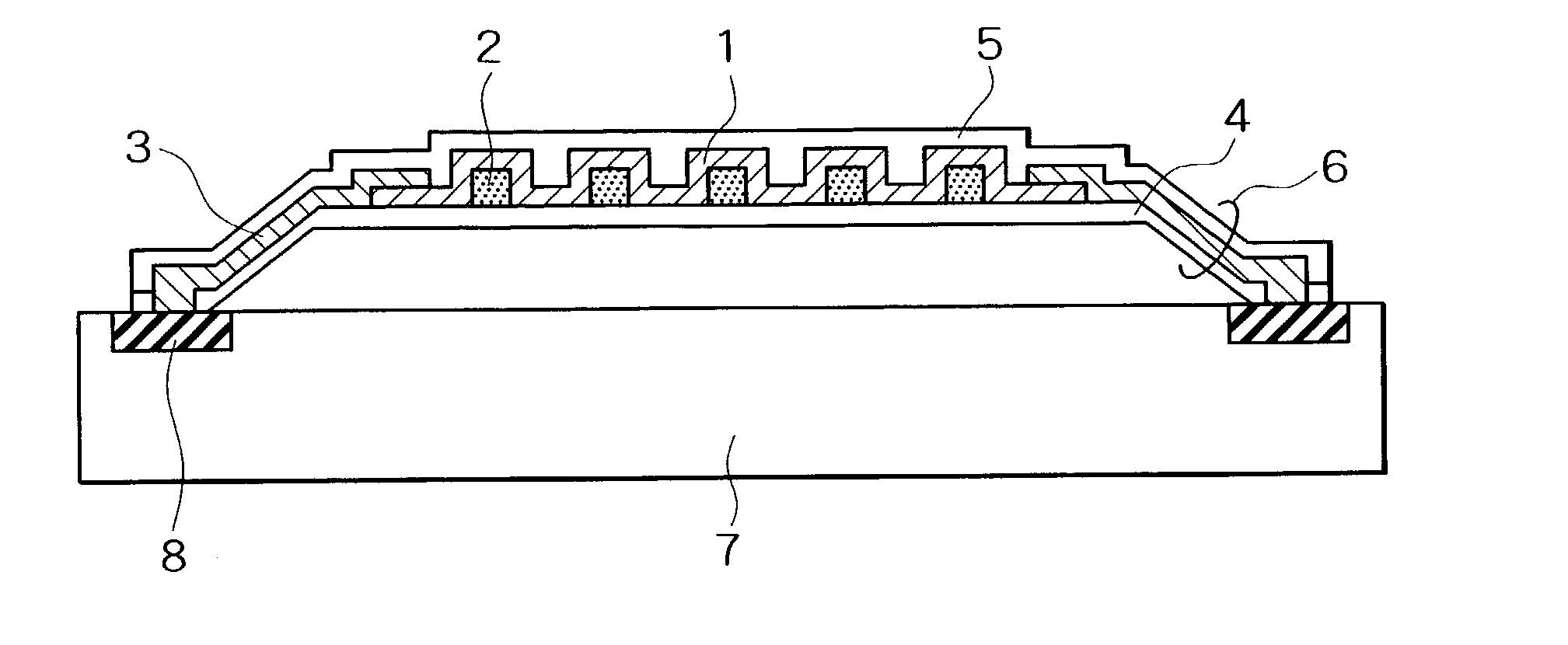
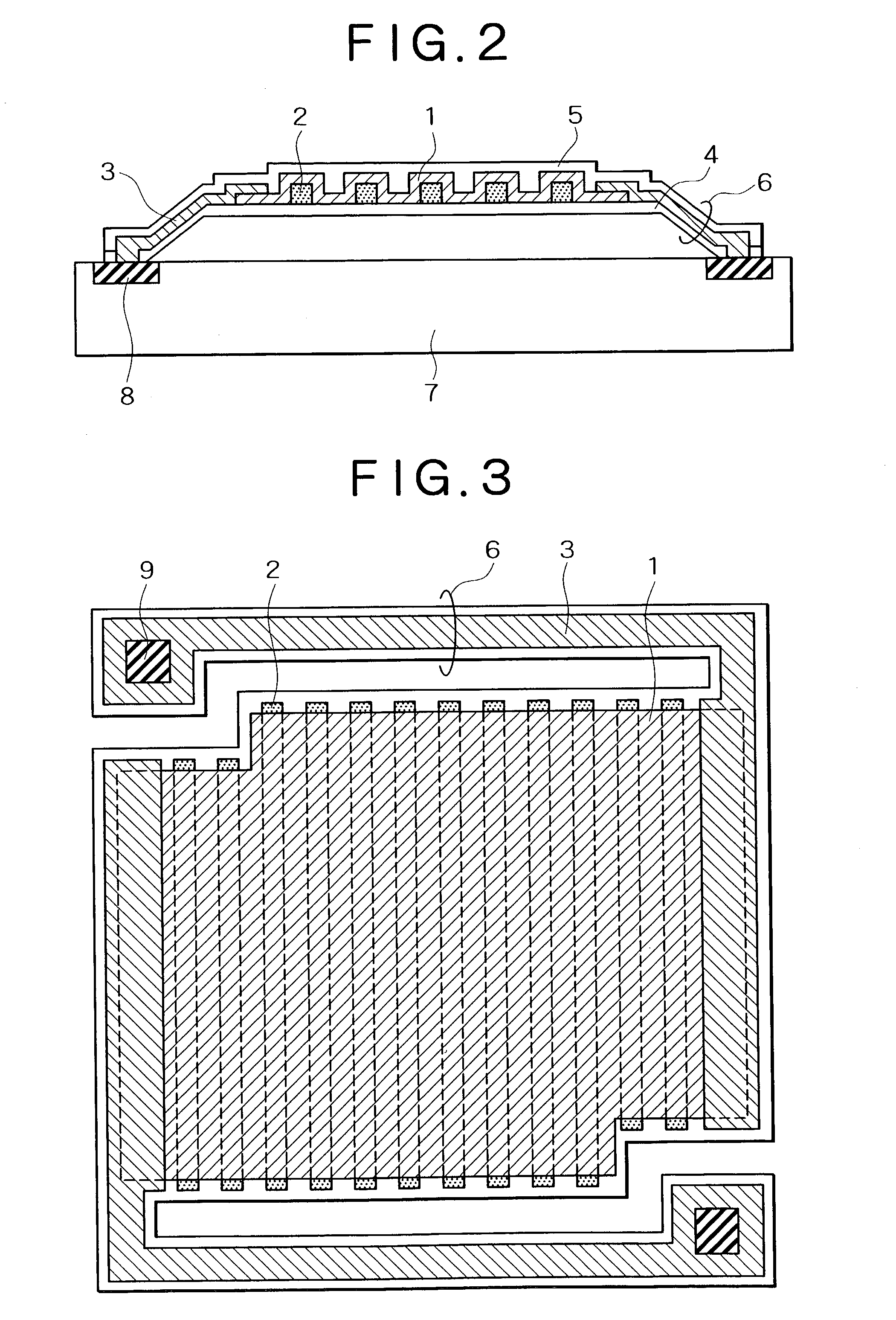
[0026] The bolometer-type infrared solid-state image sensor according to the first embodiment of the present invention will be described with reference to FIGS. 2 and 3. FIG. 2 is the schematic cross-sectional structural view of a unit pixel of the bolometer-type infrared solid-state image sensor according to the first embodiment of the present invention, and FIG. 3 is the plan view of the diaphragm that is the light-receiving section of the unit pixel. The bolometer-type infrared solid-state image sensor of the present invention is constituted by forming a plurality of the unit pixels in an array state.

[0027] Specifically, the diaphragm that is the light-receiving section stands with a self-sustaining manner in a region corresponding to one pixel of a semiconductor substrate 7, where a readout circuit has been fabricated and which is made of silicon and the like, as shown in FIG. 2, with a gap for heat isolation between the diaphragm and the semiconductor s...

second embodiment

[0033] [Second Embodiment]

[0034] Next, the bolometer-type infrared solid-state image sensor according to the second embodiment of the present invention will be described referring to FIG. 4. FIG. 4 is the plan view of the diaphragm that is the light-receiving section of the unit pixel of the bolometer-type infrared solid-state image sensor according to the second embodiment of the present invention.

[0035] In the above-described first embodiment, the stripe-shaped convex sections 2 have been provided in the direction crossing the electrical current direction of the bolometer thin film 1. However, this embodiment is characterized in that a plurality of the convex sections 2 running in the striped-shape are provided in the same direction as the electrical current direction of the bolometer thin film 1 and the bolometer thin film 1 is formed thereon. Selection of material, dimensional conditions, and the like are the same as the first embodiment described above.

[0036] With such a struct...


PUM


Abstract

A bolometer-type infrared solid-state image sensor has a plurality of infrared detecting elements provided above the substrate, which has diaphragm spacing from the substrate and supported by beams. The diaphragm has a bolometer thin film, electrodes arranged on the both end of the bolometer thin film, an upper layer protective film and a lower layer protective film, which are formed so as to sandwich and cover said bolometer thin film and the electrodes, and concave or convex sections formed on said lower layer protective film. The bolometer thin film is formed on the sides of the concave or convex sections. The beams includes wiring material and insulating protective films surrounding the wiring material.

Description

[0001] 1. Technical Field of the Invention[0002] The present invention relates to a thermal infrared solid-state image sensor having thermal isolation, particularly to a bolometer-type infrared solid-state image sensor.[0003] 2. Description of the Related Art[0004] Conventionally, the bolometer-type infrared solid-state image sensor of this kind has adopted a structure in which diaphragm simply sandwiched a bolometer thin film with an insulating protective film in a plurality of infrared detecting elements, which consist of the diaphragm spacing above a semiconductor substrate and supported by beams. Alternatively, the image sensor had comprised an infrared absorption film on a side of the insulating protective film, to which light is made incident. Then, to obtain an infrared image, the infrared detecting elements have been arranged in two-dimensionally above the semiconductor substrate and a readout circuit corresponding to the infrared detecting elements has been formed on the se...

Claims


Application Information

Patent Timeline
Patent Type & Authority Applications(United States)
IPC IPC(8): G01J5/20G01J1/02H01L27/14H01L27/146
CPCG01J5/02G01J5/20G01J5/024
Inventor TOHYAMA, SHIGERU
Owner NEC CORP
Why Eureka
Try Eureka