Fabrication method of liquid crystal display device

a liquid crystal display and fabrication method technology, applied in the field of fabrication methods of liquid crystal display devices, can solve the problems of affecting productivity, greater chances, and increased chances of misalignmen

Inactive Publication Date: 2003-11-27
LG DISPLAY CO LTD
View PDF17 Cites 20 Cited by
  • Summary
  • Abstract
  • Description
  • Claims
  • Application Information

AI Technical Summary

Problems solved by technology

The material and time consumed in each mask process directly impacts productivity.
As the number of masking processes increases, the greater chances are that misalignment will occur.
Otherwise, a major defect can occur.
Thus, misalignment of the mask can also occur regardless of the number of masking processes

Method used


Image

  • Fabrication method of liquid crystal display device
  • Fabrication method of liquid crystal display device
  • Fabrication method of liquid crystal display device

Examples


Embodiment Construction

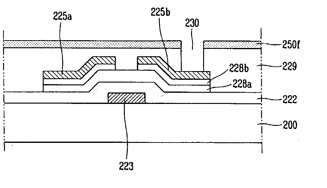
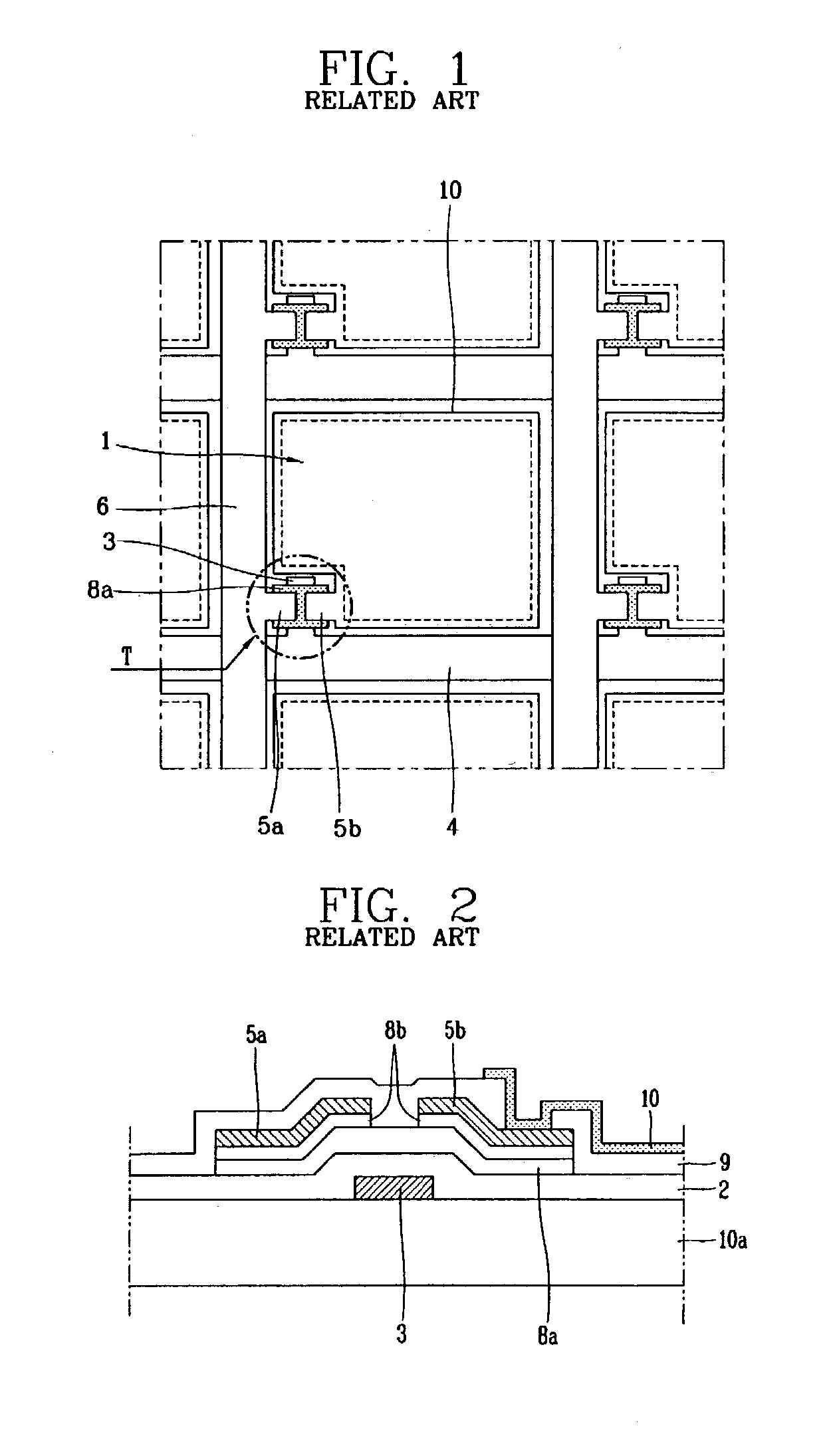
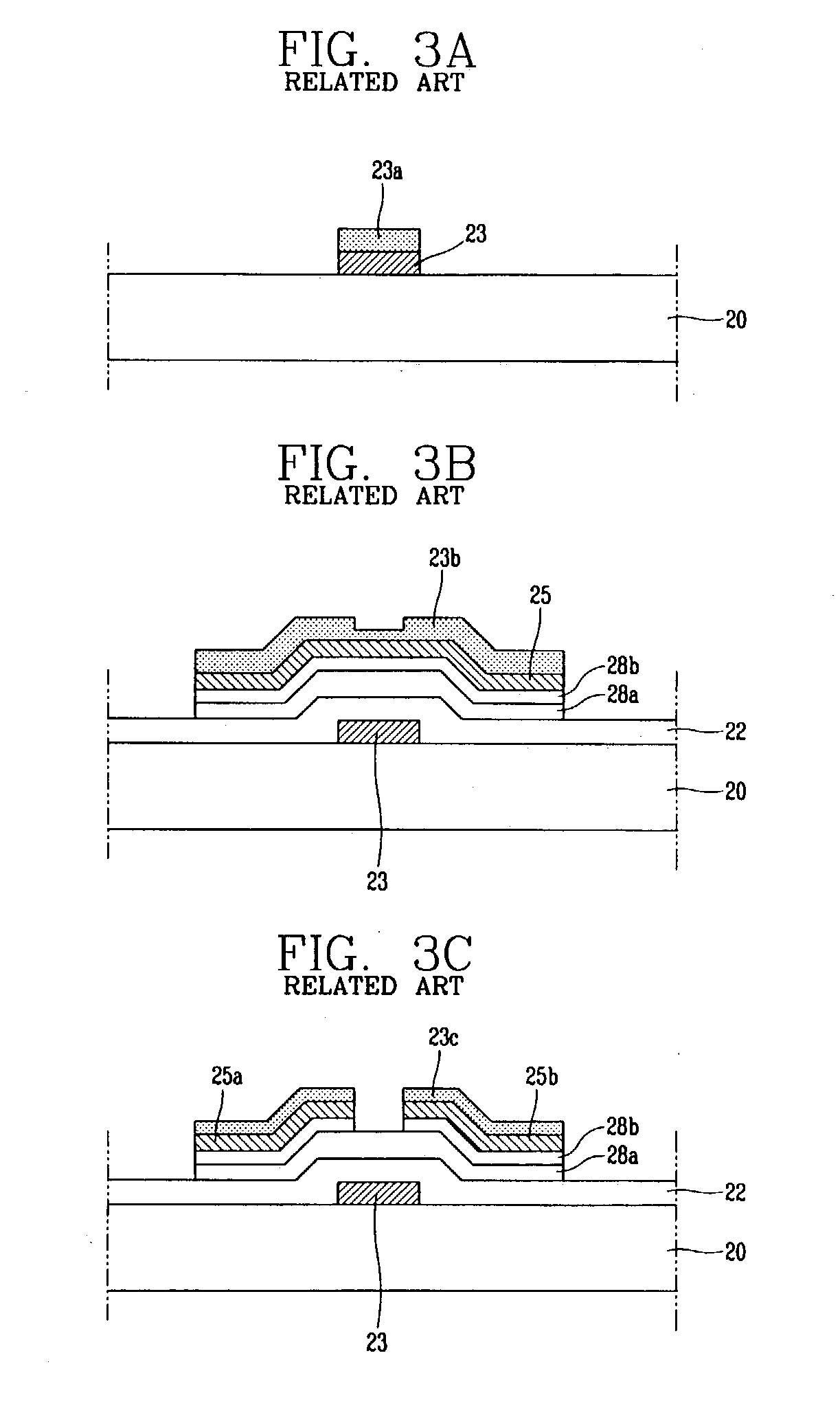
[0033] Reference will now be made in detail to the exemplary embodiments of the present invention, examples of which are illustrated in the accompanying drawings.

[0034] FIGS. 4A to 4C show a method for forming a pattern by a gravure offset printing method. As shown in FIG. 4A, a clich 100 having a groove 101 is formed, and then resist 104 is filled into the groove 101. A doctor blade 105 is then used to flatten a surface of the clich 100, so that the resist 104 is only filled into the groove 101. Then, as shown in FIG. 4B, a printing roll 110 is placed against the clich 100 and rotated across the clich 100 to transfer the resist 104 filled in the groove 101 of the clich 100 to a surface of the printing roll 110. Then, as shown in FIG. 4C, the printing roll 110 is brought into to contact with a substrate 120 and rotated across the substrate 120 to apply a resist pattern 122 onto the substrate 120. Because the resist pattern 122 is formed by using the offset printing method, the maski...


PUM

PropertyMeasurementUnit
Thicknessaaaaaaaaaa
Viscosityaaaaaaaaaa
Transparencyaaaaaaaaaa

Abstract

A method for forming a pattern includes forming a resist pattern on a printing roll, printing a multi-stepped resist pattern on an etching object layer formed on a substrate by using the printing roll and etching the etching object layer by using the printed resist pattern as a mask.

Description

[0001] This application claims the benefit of Korean Application No. 2002-28744 filed in Korea on May 23, 2002 and Korean Application No. 2002-85626 filed in Korea on Dec. 27, 2002, which are hereby incorporated by reference in their entirety.[0002] 1. Field of the Invention[0003] The present invention relates to a fabrication method of a Liquid Crystal Display (LCD) device, and more particularly, to a fabrication method of a liquid crystal display device in which a pattern is formed by using a printing method.[0004] 2. Description of the Related Art[0005] Recently, various portable electric devices, such as mobile phones, Personal Data Assistants (PDA), and notebook computers, have been developed. Such devices need a flat panel display device that is small, light weight, and power-efficient. To meet such needs, flat panel display device technologies, such as Liquid Crystal Display (LCD) technology, Plasma Display Panel (PDP) technology, Field Emission Display (FED) technology, and ...

Claims


Application Information

Patent Timeline
IPC IPC(8): G02F1/1368G03F7/00H01L21/00H01L21/28G02F1/13H01L21/3213H01L21/336H01L21/768H01L21/77H01L21/84H01L27/12H01L29/786
CPCB82Y10/00B82Y40/00G02F2001/136236H01L29/78669H01L21/67063H01L27/1214H01L29/66765G03F7/0002H01L27/1288G02F1/136236
Inventor BAEK, MYOUNG KEECHO, YONG-JINPARK, KWON SHIK
Owner LG DISPLAY CO LTD
Why Eureka
Try Eureka