Ge photodetectors

a technology of photodetectors and detectors, applied in the field of photodetectors, can solve the problems of difficult implementation of ingaas photodetectors, and achieve the effect of efficient operation and efficient operation

Inactive Publication Date: 2003-12-25
MASSACHUSETTS INST OF TECH
View PDF9 Cites 56 Cited by
  • Summary
  • Abstract
  • Description
  • Claims
  • Application Information

AI Technical Summary

Benefits of technology

0005] According to one aspect of the invention, there is provided a photodetector device. The photodetector device includes a plurality of Ge epilayers that are grown on a silicon substrate and annealed in a defined temperature range. The Ge epilayers form a tensile strained Ge layer that allows the photodetector device to operate efficiently in the C-band and L-band.
0006] According to another aspect of the invention, there is provided a method of forming a photodetector device. The method includes forming a plurality of Ge epilayers that are grown on a substrate. Moreover, the method includes annealing the Ge epilayers in a defined temperature range. Furthermore, the method includes developing a tensile strained Ge layer using the annealed Ge epilayers, the tensile strained Ge layer allowing the photodetector device to operate efficiently in the C-band and L-band.
0007] According to another aspect of the invention, there is provided a photodetector device. The photodetector device includes a plurality of SiGe epilayers that are grown on a substrate at a high temperature so as to form a SiGe structure. The SiGe layer forms a tensile strained SiGe layer by cooling to room temperature the SiGe structure using the bi-metal effect. The tensile strained SiGe layer allows the photodetector device to operate efficiently in the C-band and L-band.
0008] According to another aspect of the invention, there is provided a method of forming a photodetector device. The method includes growing a plurality of SiGe epilayers on a silicon substrate at a high temperature so as to form a SiGe structure. Furthermore, the method includes forming a tensile strained SiGe layer by cooling to room temperature the SiGe structure using the bi-metal effect. The tensile strained SiGe layer allows the photodetector device to operate efficiently in the C-band and L-band.

Problems solved by technology

InGaAs photodetectors are not easy to implement on a silicon chip, since InGaAs is a III-V compound semiconductor.

Method used


Image

  • Ge photodetectors
  • Ge photodetectors
  • Ge photodetectors

Examples


Embodiment Construction

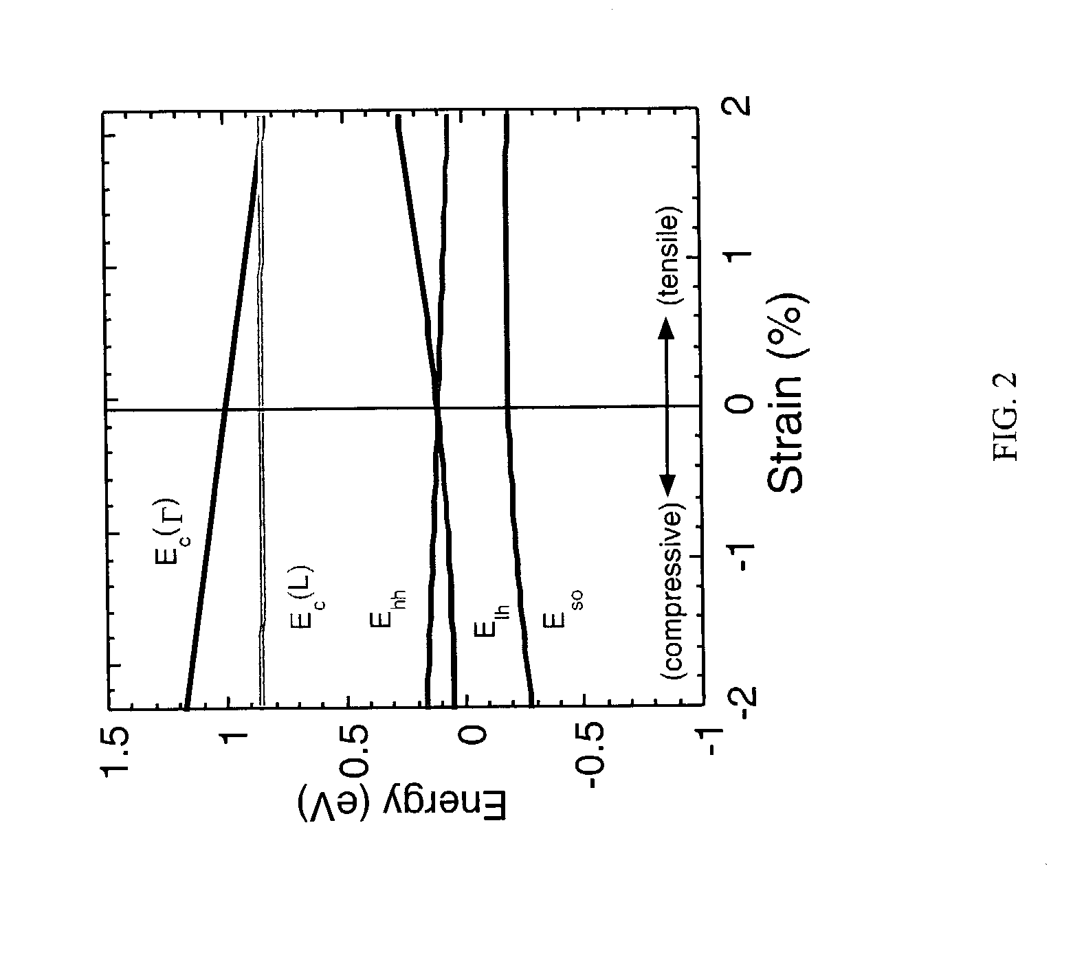
[0015] Ge is an indirect semiconductor whose bandgap is 0.667 eV corresponding to 1850 nm. Because of indirect bandgap characteristics, the absorption coefficient is small, approximately 100 cm.sup.-1 depending on the wavelength. The direct bandgap of Ge is 0.8 eV corresponding to 1550 nm. Thus, the photodetector performance of Ge is marginally good in the C-band but, is poor in the L-band. To overcome the drawback of Ge, various attempts have been used, such as GeSn alloy, to decrease the bandgap.

[0016] One goal in Ge photodetectors is to shrink the bandgap to cover the C- and L-bands with high efficiency. The invention uses tensile strain to accomplish this task.

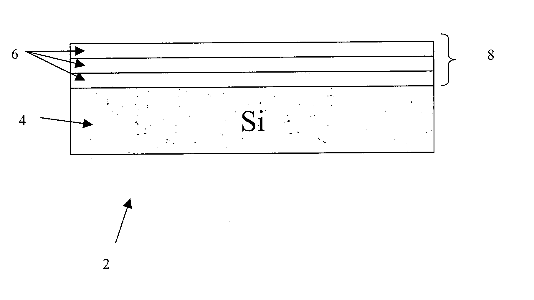
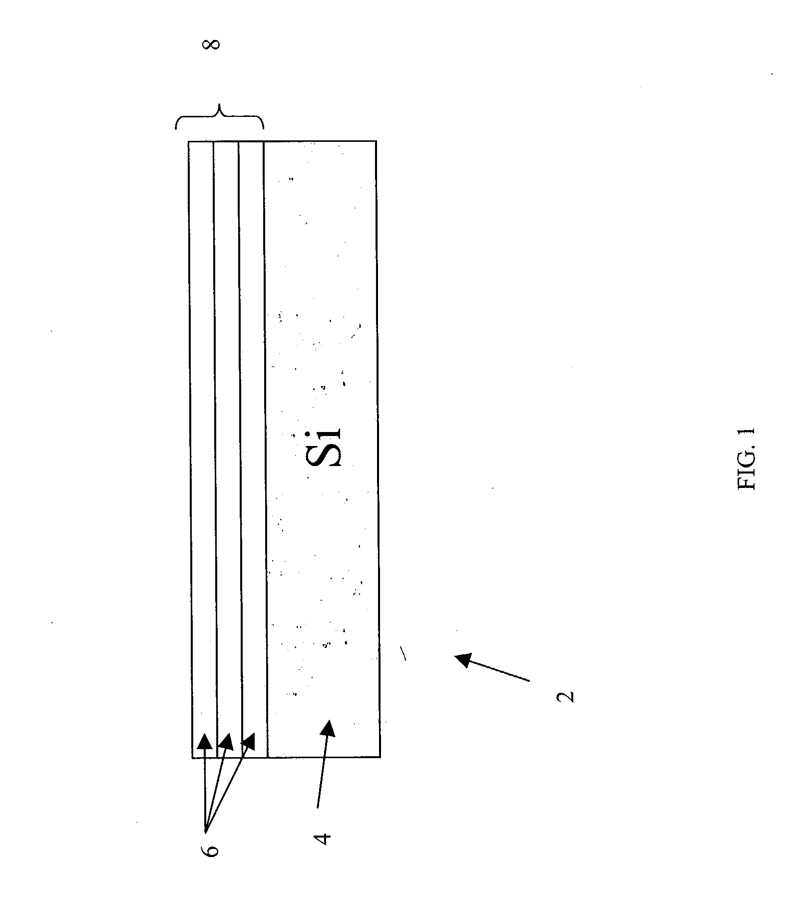
[0017] FIG. 1 is schematic block diagram illustrating the techniques used to create a Ge photodetector 2 using a tensile strained Ge layer 8. The Ge photodetector is formed on a Si wafer. This is ideal for realizing Si-based optoelectronic circuits as well as optical interconnection in Si-LSIs. In spite of a large lattice ...


PUM


Abstract

A photodetector device includes a plurality of Ge epilayers that are grown on a substrate and annealed in a defined temperature range. The Ge epilayers form a tensile strained Ge layer that allows the photodetector device to operate efficiently in the C-band and L-band.

Description

PRIORITY INFORMATION[0001] This application claims priority from provisional application Ser. No. 60 / 389,819 filed Jun. 19, 2002, which is incorporated herein by reference.BACKGROUND OF THE INVENTION[0002] The invention relates to the field of photodetectors, and in particular to monolithically integrated Ge photodetectors on Si.[0003] Photodetectors are fundamental devices that convert optical signals into electric signals. Fiber optical communication employs 1300 and 1550 nm wavelengths because of low attenuation coefficients of silica fibers. Er doped fiber amplifiers emphasize the importance of 1550 nm because of the direct amplification of optical signals without converting to electric signals. The amplification range between 1530-1560 nm is referred to as C-band, and the recently extended amplification range between 1570-1608 nm is referred to as L-band. The photodetectors for 1550 nm detection have so far been InGaAs photodetectors, since InGaAs is a direct semiconductor whos...

Claims


Application Information

Patent Timeline
Patent Type & Authority Applications(United States)
IPC IPC(8): H01L21/00H01L27/04H01L31/10H01L27/14H01L27/146H01L27/15H01L29/06H01L31/028H01L31/18
CPCH01L21/02381H01L21/0245H01L21/02532H01L21/0262H01L27/146Y02P70/521H01L31/1808H01L31/1864H01L31/1872Y02E10/50Y10S438/933H01L31/103Y02P70/50H01L31/028H01L27/14H01L31/18H01L27/04
Inventor WADA, KAZUMIKIMERLING, LIONEL C.ISHIKAWA, YASUHIKOCANNON, DOUGLAS D.LIU, JIFENG
Owner MASSACHUSETTS INST OF TECH
Why Eureka
Try Eureka