Light emitting device and lighting apparatus using the same

a technology of light emitting devices and lighting apparatuses, which is applied in the direction of semiconductor devices for light sources, lighting and heating devices, fixed installations, etc., can solve the problems of incandescent bulbs, filaments suffer from a relatively short service life, and low efficiency

Inactive Publication Date: 2004-02-12
SHIN-ETSU HANDOTAI CO LTD
View PDF10 Cites 52 Cited by
  • Summary
  • Abstract
  • Description
  • Claims
  • Application Information

AI Technical Summary

Problems solved by technology

Incandescent bulbs which illuminate based on resistance heat generation of the filaments suffer from a relatively short service life and a low efficiency due to a large Joule heat loss.
They are also disadvantageous in that a large amount of infrared radiation emitted together with visible light during the light emission, and this considerably raises temperature of the light source.
Natural combustion lights suffer from further shorter service life, and require labor-consuming maintenance works due to production of large amount of combustion products such as soot and carbon dioxide.
although power consumption is smaller than that of incandescent bulbs, it is still not ignorable because high voltage is necessary;
phosphorescent light obtained from calcium halophosphates is substantially white, but the spectrum thereof largely differs from that of natural light (sunlight), and thus raises a problem of color rendering properties.
Light emitting diodes, however, have only limited emission wavelength regions which are governed by band gap values of semiconductors to be used, and this makes it impossible to obtain an emission spectrum covering a wide visible light band, and emission from most of them is only almost monochromatic.
There have thus been almost no applications of the light emitting diodes in the field of general lighting where color rendering properties are required.
This kind of devices, however, raise a problem that they can produce only extremely discrete emission spectra characterized by sharp peaky bright lines, and consequently that they are poor in co

Method used


Image

  • Light emitting device and lighting apparatus using the same
  • Light emitting device and lighting apparatus using the same
  • Light emitting device and lighting apparatus using the same

Examples


Embodiment Construction

[0067] The following paragraphs will describe embodiments of the invention referring to the attached drawings.

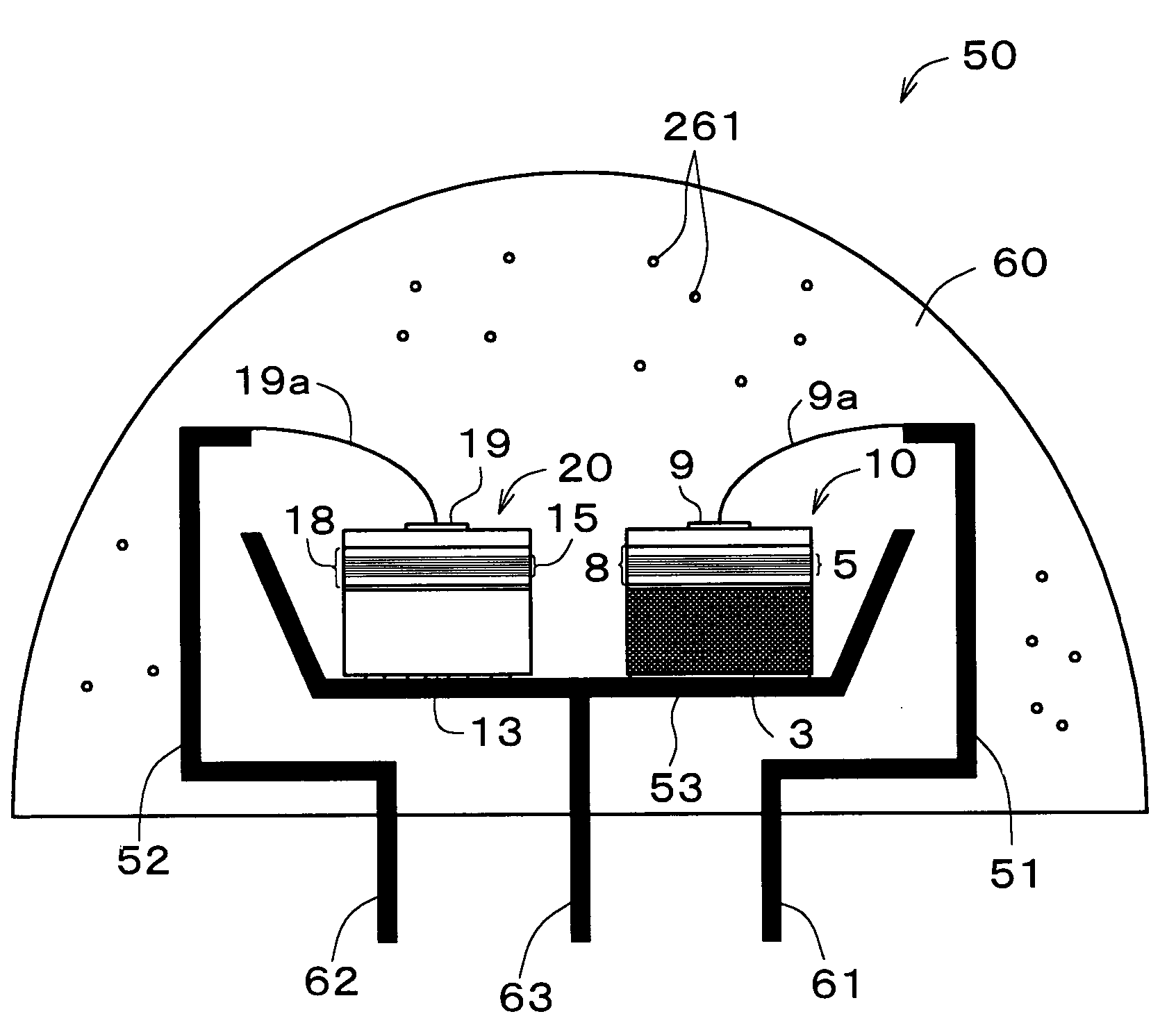
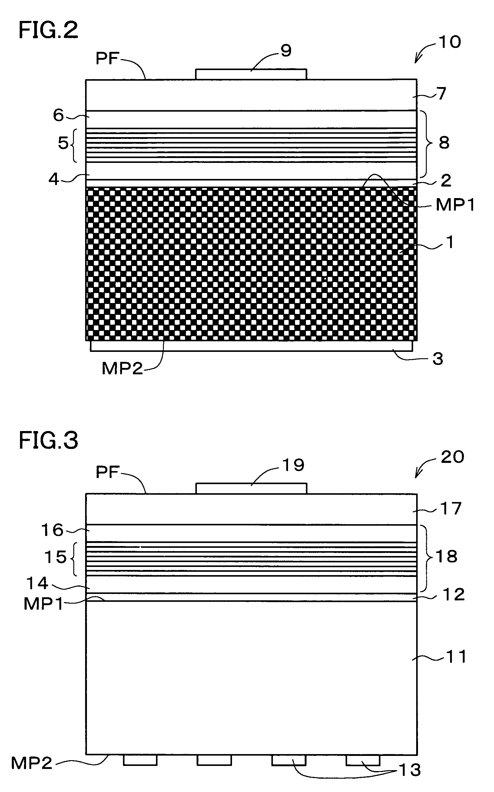
[0068] FIG. 1 is a schematic drawing of an exemplary light source for illumination using a light emitting device according to one embodiment of the invention. The light source for illumination 50 has light emitting devices 10, 20 according to a concept of the invention. The light emitting devices 10, 20 are specifically a first device 10 and a second device 20, where active layers (see FIGS. 2 and 3) of double hetero light emitting layer portions 8, 18 (simply referred to as "light emitting layer portions", hereinafter), which are composed of compound semiconductors, are respectively configured so as to include a plurality of emission unit layers differing from each other in the band gap energy. Emission wavelength of the emission unit layers of the first device 10 is set within a range from 520 nm to 700 nm, both ends inclusive, and that of the second device 20 is set withi...


PUM


Abstract

A light emitting device capable of readily produce a pseudo-continuous spectrum covering a wide wavelength regions at low costs, and of totally solving various problems which have resided in the conventional light sources, and a lighting apparatus using this device is provided. The light emitting device 10 is configured so that an active layer in a double hetero light emitting layer portion composed of compound semiconductors comprises a plurality of emission unit layers differing from each other in band gap energy, and so as to emit a simulatively synthesized light having a pseudo-continuous spectrum ensuring an emission intensity of 5% or more of a peak intensity over a wavelength region of 50 nm or more.

Description

[0001] This application claims the priorities of Japanese Patent Application Nos. 2002-224250 filed on Jul. 31, 2002 and 2003-061684 filed on Mar. 7, 2003.[0002] 1. Field of the Invention[0003] This invention relates to a light emitting device and a lighting apparatus using the light emitting device.[0004] 2. Description of the Related Art[0005] Incandescent bulbs have long been used as a light source for lighting, and in more earlier times before the incandescent bulbs are invented, natural combustion light such as candles or torches had been used. Incandescent bulbs which illuminate based on resistance heat generation of the filaments suffer from a relatively short service life and a low efficiency due to a large Joule heat loss. They are also disadvantageous in that a large amount of infrared radiation emitted together with visible light during the light emission, and this considerably raises temperature of the light source. Natural combustion lights suffer from further shorter s...

Claims


Application Information

Patent Timeline
IPC IPC(8): F21V23/00F21S2/00F21S8/00F21S10/04F21V5/04F21V23/02F21Y101/02H01L25/075H01L33/00H01L33/06H01L33/30H01L33/32H01L33/48H01L33/56
CPCF21K9/17F21K99/00H01L2224/73265H01L2224/48247H01L2224/48091H01L2224/32245F21W2121/00F21S6/001F21S8/04F21S10/04F21W2131/109F21Y2101/02H01L25/0753H01L33/06H01L33/483H01L33/62H01L2924/09701H01L2933/0091H01L2924/00012H01L2924/00F21K9/232F21Y2115/10H01L33/08H01L2924/00014
Inventor YAMADA, MASATOTAKAHASHI, MASANOBU
Owner SHIN-ETSU HANDOTAI CO LTD
Why Eureka
Try Eureka