Junction field-effect transistor

Inactive Publication Date: 2004-04-08
ROHM CO LTD
View PDF0 Cites 14 Cited by
  • Summary
  • Abstract
  • Description
  • Claims
  • Application Information

AI Technical Summary

Benefits of technology

[0005] The present invention has been made in order to solve the foregoing problem, and it is an object thereof to provide a high-gain junction field-effect transistor which has low variation in characteristics by reducing the junction-FET drain-source leak current I.sub.dss to a small, stable value.
[0007] This structure forms a diffusion region having a conductivity type different from the drain and source regions at the side of the drain region close to the gate region in a semiconductor layer surface where impurity concentration variation tends to occur and leak current readily flows, thus operating as an FLR (field limiting ring). A depletion layer is thus formed at the surface of the epitaxially grown semiconductor layer of the drain and source regions along with the gate region, thereby preventing current flow. Thus almost no leak current flows near the surface of the semiconductor layer. As a result, the leak current I.sub.dss between the drain and the source, where the gate and the source are connected, can be suppressed to a stable, small value. This brings about a stable gain and greatly improves the performance of the FET.

Problems solved by technology

This results in a problem that there is gain decrease or variation in characteristics depending upon the manufacture lot, thus making it impossible to obtain a junction FET having a high gain with stable characteristics.

Method used


Image

  • Junction field-effect transistor
  • Junction field-effect transistor
  • Junction field-effect transistor

Examples


Embodiment Construction

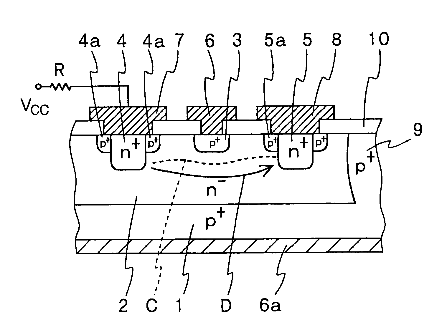
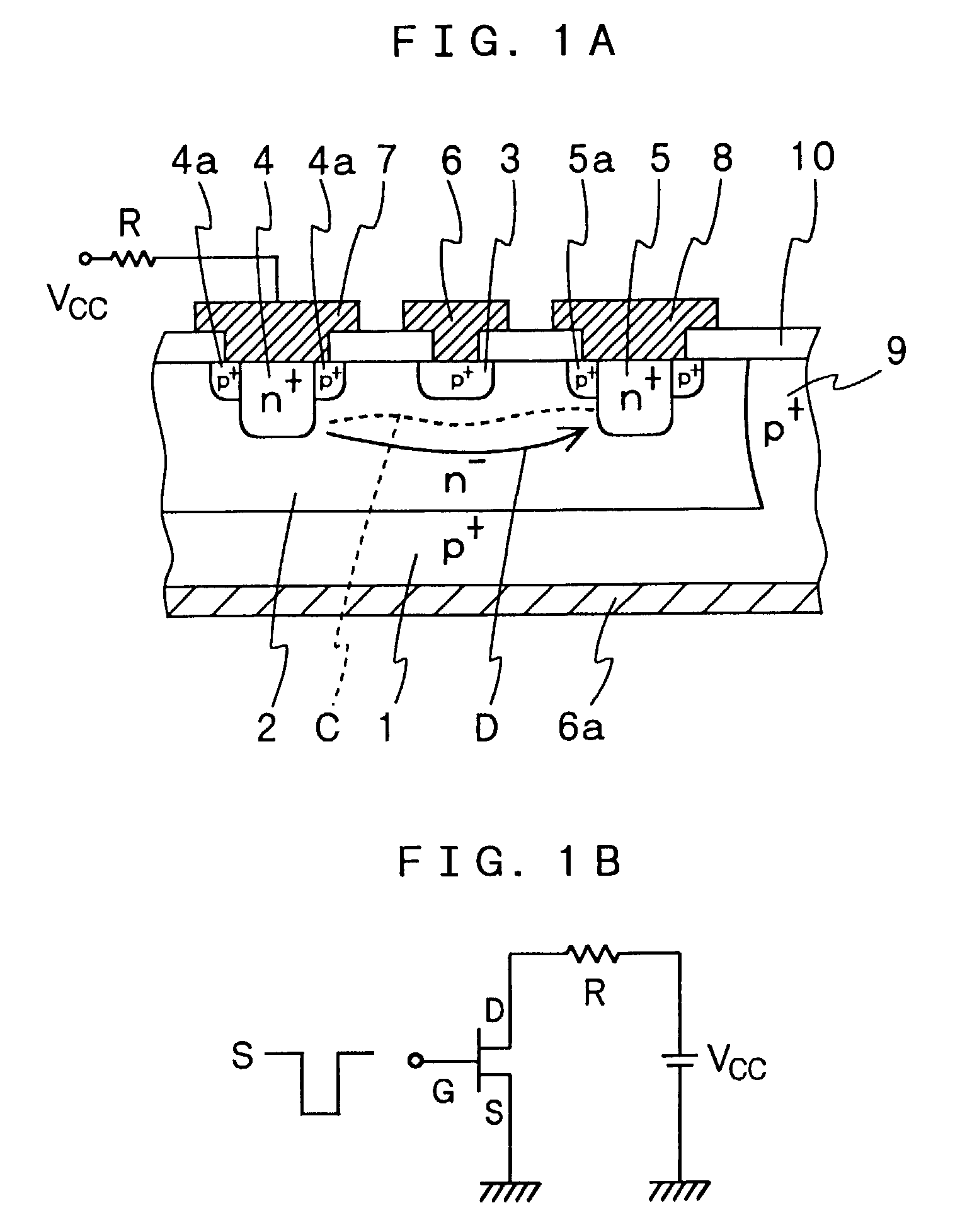
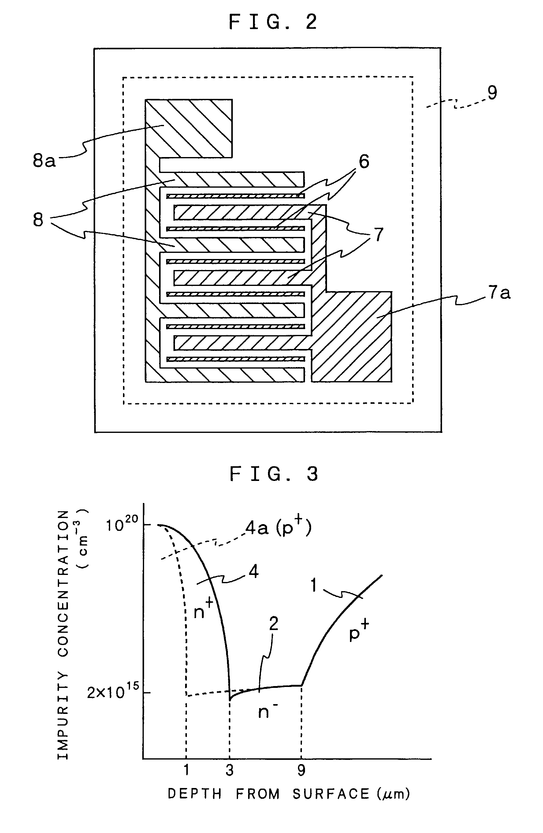
[0013] Explanation will be now made of a junction field-effect transistor of the present invention with reference to the drawings. The junction field-effect transistor of the invention has a gate region 3 of a second conductivity type (p-type) on the surface of a first conductivity type (n-type) semiconductor layer 2, and n.sup.+-type drain region 4 and source region 5 sandwiching the gate region 3 on the surface of the n-type semiconductor layer 2, as shown in the cross sectional explanatory view of one embodiment of FIG. 1A, thus forming a junction field-effect transistor. A p-type diffusion layer 4a is formed on the surface of the n-type semiconductor layer 2 at least on the side of the drain region 4 close to the gate region 3. A drain electrode 7 is formed so that it is connected with the p-type diffusion region 4a.

[0014] The example shown in FIG. 1A is an example having a drain and a source on the respective sides of each stripe-formed gate as shown in a plan explanatory view ...


PUM


Abstract

A junction field-effect transistor is formed by providing a p-type gate region in a surface of an n-type semiconductor layer and n-type drain and source regions sandwiching the gate region on the surface of the n-type semiconductor layer. A p-type diffusion region is formed at least in the region on the side of the drain close to the gate region on the surface of the n-type semiconductor layer. A drain electrode is formed so that it contacts with the p-type diffusion region. As a result, the junction FET can be reduced in drain-source leak current I.sub.dss to a small, stable value. Thus, a high-gain junction field-effect transistor is obtained which has small variation in performance among actual units manufactured.

Description

FIELD OF THE INVENTION[0001] This invention relates to junction a field-effect transistor and, more particularly, to a junction field-effect transistor having a gate-source connection in which drain-source leak current I.sub.dss is decreased, thereby improving FET performance in such factors as gain.BACKGROUND OF THE INVENTION[0002] The junction FET is formed with a p.sup.+-type gate region 23 diffused on an n.sup.--type semiconductor layer 22 epitaxially grown, for example, on a p.sup.+-type semiconductor substrate 21, and an n.sup.--type drain region 24 and source region 25 diffused on both sides thereof, as shown in the cross sectional explanatory view FIG. 5A. It is noted that the semiconductor substrate 21 is connected to the gate electrode 26 and not-shown p.sup.+-type diffusion region (channel stop) through an interconnection to have, on a back surface thereof, a gate electrode 26a for connection onto a die pad. In FIG. 5A, 26 is a gate electrode, 27 a drain electrode, 28 a s...

Claims


Application Information

Patent Timeline
IPC IPC(8): H01L29/417H01L29/423H01L29/74H01L29/808H01L31/111
CPCH01L29/41725H01L29/808H01L29/42316
Inventor SAKAMOTO, KAZUHISA
Owner ROHM CO LTD
Why Eureka
Try Eureka