Copper sputtering targets and methods of forming copper sputtering targets

a technology of copper sputtering and copper sputtering target, which is applied in the direction of vacuum evaporation coating, transportation and packaging, coatings, etc., can solve the problems of increasing the overall average grain size, non-uniform microstructure, and relatively low yield strength

Inactive Publication Date: 2004-04-15
HONEYWELL INT INC
View PDF74 Cites 61 Cited by
  • Summary
  • Abstract
  • Description
  • Claims
  • Application Information

AI Technical Summary

Problems solved by technology

However, the high temperatures utilized during bonding of the copper target to the backing plate often results in abnormal grain growth resulting in non-uniformity of microstructure and an increase in overall average grain size.
Conventional high-purity copper targets typically have an average grain size greater than 50 microns which can result in relatively low yield strength.
The resulting grain size and structural non-uniformity of conventionally formed high-purity copper sputtering targets can detrimentally affect the quality of sputter-deposited high-purity copper films and interconnects.
In addition to the resulting large grain size and anomalous grain growth that can result during bonding processes, diffusion bonded copper targets are often plagued by problems such as burn through and short target life.
Additionally, bonding processes can be complicated and time consuming.
Another draw back to alloying can be potential defects such as formation of second phase precipitates or segregation.
Although treatment of conventional materials for reduction or removal of precipitates or segregation defects may be possible in some instances, such treatment typically includes high temperatures which can result in extremely large grain sizes (greater than 150 microns).
However, the remaining defects can still affect the quality of sputtered films.
Such low temperature or absence of anneal can result in a blank having an average grain size of less than about 1 micron.

Method used


Image

  • Copper sputtering targets and methods of forming copper sputtering targets
  • Copper sputtering targets and methods of forming copper sputtering targets
  • Copper sputtering targets and methods of forming copper sputtering targets

Examples


example 2

Production of Copper Alloy Monolithic Sputtering Targets

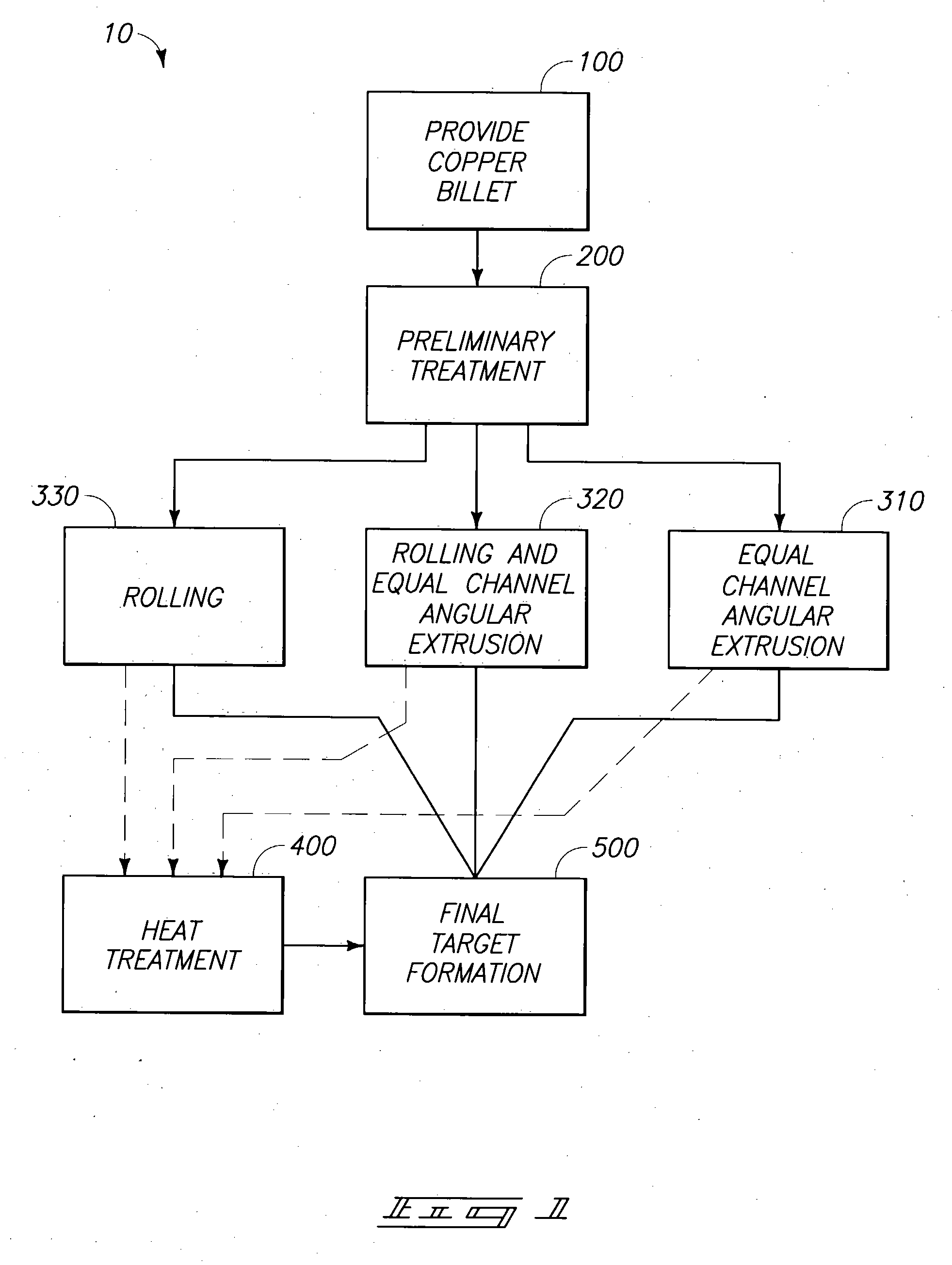
[0089] Copper alloy billets having less than 10% of Ag, Sn, Al, or Ti are heated and maintained at a temperature of about 900.degree. F. to about 150.degree. F. for about 45 minutes. The billets are then hot forged to produce a final reduction of at least about 50%. Some of forged billets (depending on the alloy) are reheated for at least 10 minutes during the forging. After the final forging, the forged billets are immediately water quenched. The forged blocks are cold-rolled to a reduction of at least about 60% to form a blank which is recrystallized by heating to a temperature of from about 750.degree. F. to about 1200.degree. F. for 120 minutes. The recrystallized blanks are machined to form monolithic targets. Each of the targets has an average grain size of from about 15 microns to about 50 microns.

[0090] A specific target having copper alloyed with 0.3 atomic % Al was formed from a billet having a six inch diameter and a...

example 3

Production of Copper Alloy Diffusion Bonded Sputtering Targets

[0092] Copper alloy billets are provided and processed as described in example 2 with the exception that the cold-rolling was conducted to a reduction of at least about 50%. The cold-rolled blanks are bonded to CuCr backing plates at a bonding temperature of about 450.degree. C. for about 120 minutes. Recrystallization of the alloy occurs during the bonding. The bonded targets have a grain size of less than about 30 microns and a bond strength of up to about 30 ksi.

example 4

Production of High-Purity Copper Sputtering Targets Utilizing ECAE

[0093] Copper billets of cast copper having a purity of at least 99.9999% are provided. The high-purity copper billets are hot-forged at a temperature of least about 500.degree. C. with a reduction in height of at least about 40% to form forged blocks. The forged blocks are solutionized by heating the blocks to a temperature of at least about 500.degree. C. which is maintained for at least about 1 hour. The solutionized blocks are water quenched immediately after the heat treatment and are extruded utilizing from four to six passes of equal channel angular extrusion (ECAE) in accordance with route D (90 degree rotation of the blocks between successive passes) to produce a sub-micron microstructure. Intermediate annealing at a temperature of from about 125.degree. C. to about 225.degree. C., and for a time of at least about 1 hour is performed between some or all of the ECAE passes. The extruded high-purity copper bloc...


PUM

PropertyMeasurementUnit
grain sizeaaaaaaaaaa
yield strengthaaaaaaaaaa
grain sizeaaaaaaaaaa

Abstract

The invention includes a copper-comprising sputtering target. The target is monolithic or bonded and contains at least 99.99% copper by weight and has an average grain size of from 1 micron to 50 microns. The copper-comprising target has a yield strength of greater than or equal to about 15 ksi and a Brinell hardness (HB) of greater than about 40. The invention includes copper alloy monolithic and bonded sputtering targets consisting essentially of less than or equal to about 99.99% copper by weight and a total amount of alloying element(s) of at least 100 ppm and less than 10% by weight. The targets have an average grain size of from less than 1 micron to 50 microns and have a grain size non-uniformity of less than about 15% standard deviation (1-sigma) throughout the target. The invention additionally includes methods of producing bonded and monolithic copper and copper alloy targets.

Description

RELATED PATENT DATA[0001] This patent is a continuation in part of U.S. patent application Ser. No. 09 / 465,492 which was filed on Dec. 16, 1999 and which is herein incorporated by reference. This patent further claims benefit of priority under 35 U.S.C. .sctn.119 to U.S. Provisional Patent Serial No. 60 / 396,544, which was filed Jul. 16, 2002, and to U.S. Provisional Patent Serial No.: Not Yet Assigned, entitled Copper Sputtering Targets and Methods of Forming Copper Sputtering Targets, which was filed May 15, 2003.[0002] The invention pertains to copper-comprising monolithic sputtering targets and copper-comprising bonded sputtering targets. The invention additionally pertains to methods of forming copper-comprising monolithic and bonded sputtering targets.[0003] High-purity copper sputtering targets and copper alloy sputtering targets are currently used in a variety of applications including, for example, fabrication of integrated circuits. The quality of copper-comprising structur...

Claims


Application Information

Patent Timeline
Patent Type & Authority Applications(United States)
IPC IPC(8): B21J5/00B21C23/01C22C9/01C22C9/02C22C9/04C22C9/05C22C9/06C22C9/10C22F1/00C22F1/08C23C14/34H01L21/285
CPCB21C23/001B21C23/01Y10T428/12118C23C14/3414C22F1/08C23C14/14C23C14/548
Inventor SEGAL, VLADIMIR M.YI, WUWENFERRASSE, STEPHANEWU, CHI TSESTROTHERS, SUSAN D.ALFORD, FRANK A.WILLETT, WILLIAM B.
Owner HONEYWELL INT INC
Why Eureka
Try Eureka