Nonvolatile semiconductor memory having three-level memory cells and program and read mapping circuits therefor

a technology of memory cells and nonvolatile semiconductors, applied in static storage, digital storage, instruments, etc., can solve the problems of affecting the reliability of memories using four-level memory cells, slow random access time for this type of sensing technique, and functional failur

Inactive Publication Date: 2004-04-29
WINBOND ELECTRONICS CORP
View PDF21 Cites 108 Cited by
  • Summary
  • Abstract
  • Description
  • Claims
  • Application Information

AI Technical Summary

Problems solved by technology

Disadvantageously, two consecutive comparisons makes the random access time slower for this type of sensing technique, relative to the parallel sensing technique of FIG. 4.
The reliability of memories using four-level memory cells can be adversely affected because of the smal

Method used


Image

  • Nonvolatile semiconductor memory having three-level memory cells and program and read mapping circuits therefor
  • Nonvolatile semiconductor memory having three-level memory cells and program and read mapping circuits therefor
  • Nonvolatile semiconductor memory having three-level memory cells and program and read mapping circuits therefor

Examples


Embodiment Construction

[0043] A memory has an array of preferably three-level memory cells, comparators for detecting the levels actually stored in selected cells, and a bit mapping circuit that maps the cells to bits using a partial function.

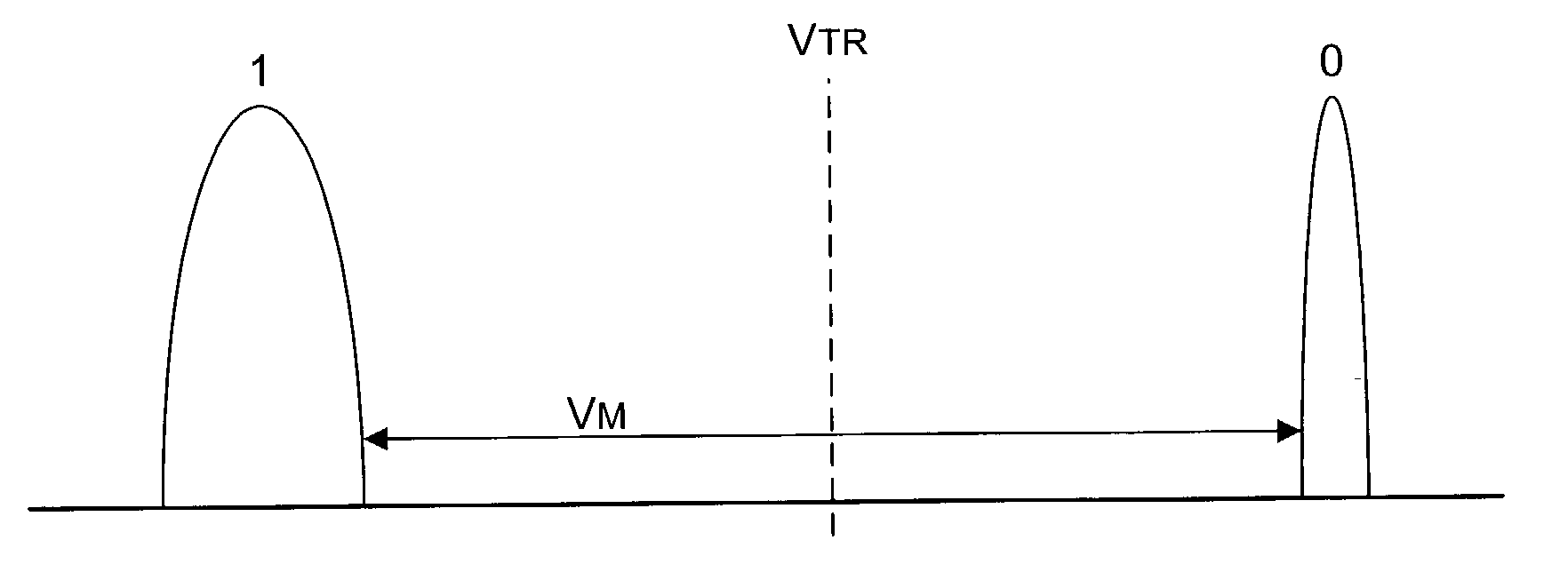
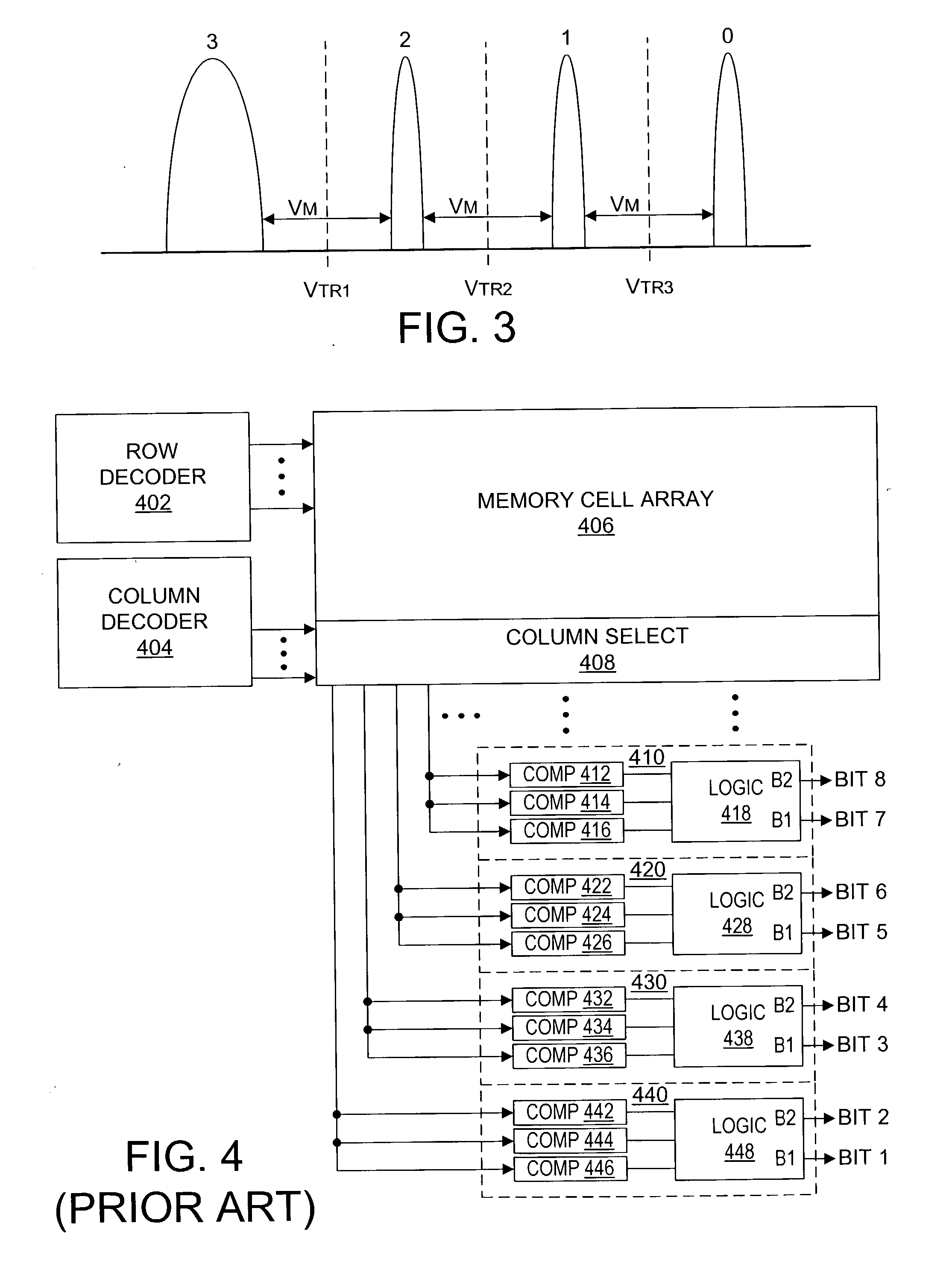
[0044] FIG. 5 is a graph showing an illustrative threshold voltage distribution for a three-level memory cell. The voltage margin V.sub.M between the states 0 and 1 and the states 1 and 2 is about 1.25 volts, assuming that the threshold voltage V.sub.T distribution width for state 1 is 0.5 volts, and that the threshold voltage gap between state 0 and state 2 is 3 volts. If the sensing threshold reference voltage V.sub.TRis positioned in the middle between two adjacent states, the difference between the edge of each cell's threshold voltage distribution and the sensing threshold reference voltage V.sub.TR (the "sensing margin") is 0.625 volts.

[0045] As is apparent from a comparison of the graph of FIG. 5 with the graph of FIG. 3, the voltage margin V.sub.M of the thre...


PUM


Abstract

A memory uses multiple threshold levels in a memory cell that are not a power of two, and further uses a cell mapping technique wherein the read mapping is only a partial function The domain of read states for a single three-level memory cell, for example, has three states, but only two of them can be uniquely mapped to a bit. The domain of read states for two three-level memory cell, for example, has nine states, but only eight of them can be uniquely mapped to three bits. Although the read mapping is only partial, the voltage margin for the three-level memory cells is larger that the voltage margin available in the commonly used four-level memory cells. This increased voltage margin facilitates memory cell threshold voltage sensing, thereby increasing the reliability of the memory. Memory reliability may be further improved by increasing the voltage margin between the memory cell 0 state and the 1 state relative to the voltage margin between the 1 state and the 2 state, which more effectively accommodates charge loss from the 0 state through electron leakage. Asymmetrical read and program mapping may also be used to improve read reliability in the presence of ground noise or VCC noise.

Description

[0001] 1. Field of the Invention[0002] The present invention relates to nonvolatile semiconductor memory, and more particularly to nonvolatile semiconductor memory having three-level memory cells and program and read mapping circuits therefor.[0003] 2. Description of the Related Art[0004] Nonvolatile semiconductor memory array retains stored data when power is removed. Many different types of data cells suitable for nonvolatile memory are known, including a class of single transistor devices that are based on the storage of charge in discrete trapping centers of a dielectric layer of the structure, and another class of devices that are based on the storage of charge on a conducting or semiconducting layer that is completely surrounded by a dielectric, typically an oxide. The trapped charge establishes the threshold voltage, or V.sub.T, of the device, which is sensed when the memory is read to determine the data stored therein.[0005] An illustrative well known type of compact floatin...

Claims


Application Information

Patent Timeline
IPC IPC(8): G11C11/56G11C16/26
CPCG11C7/1006G11C11/5628G11C2211/5641G11C16/26G11C11/5642
Inventor PARK, EUNGJOON
Owner WINBOND ELECTRONICS CORP
Why Eureka
Try Eureka