

Plasma processing device and plasma processing method
a plasma processing and plasma technology, applied in the direction of electrical equipment, basic electric elements, electric discharge tubes, etc., can solve the problems of difficult gas optimization, process with a sufficiently high uniformity may not be executed, and process uniformity may not be lowered, so as to achieve high uniformity and high uniformity
- Summary
- Abstract
- Description
- Claims
- Application Information
AI Technical Summary
Benefits of technology
Problems solved by technology
Method used
Image

Examples
first embodiment
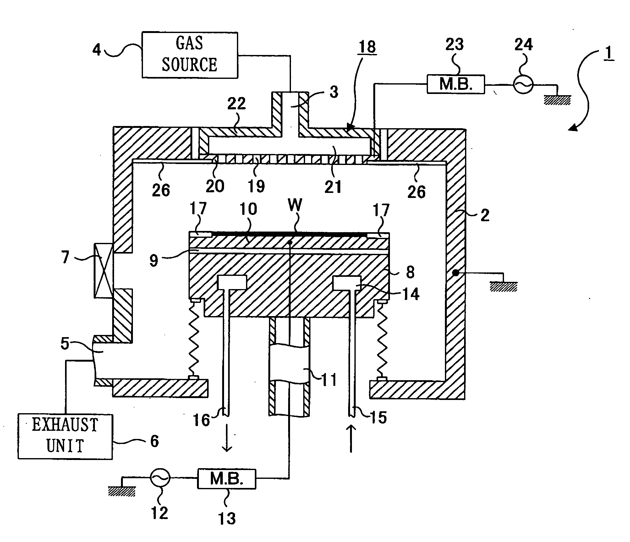
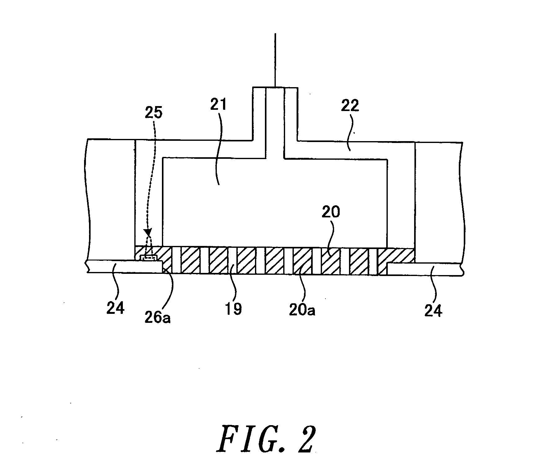
[0099] As described above, the first embodiment takes such a structure that the electrode plate 20 is formed into a projection type and the exposed surface of the electrode plate 20 and the major surface of the shield ring 26 form a flat surface. This structure eliminates the step between the electrode plate 20 and the shield ring 26, and can reduce or eliminate the disturbance of the process gas above the wafer W. Accordingly, the pressure above the wafer W becomes nearly uniform on the entire top surface so that a process with high uniformity can be performed on the entire top surface. Further, the pressure above the wafer W can be kept at a relatively low pressure so that a highly reliable process with suppressed generation of voids can be executed.
[0100] In the first embodiment, the height of the projection 20a of the electrode plate 20 is approximately equal to the thickness of the shield ring 26 and the electrode plate 20 and the shield ring 26 form substantially the same surf...
second embodiment
[0101] The second embodiment of the invention will be discussed below. A plasma process system 1 according to the second embodiment has nearly the same structure as the plasma process system 1 of the first embodiment illustrated in FIG. 1. FIG. 6 shows an enlarged diagram of near the upper and lower electrodes of the second embodiment. In the diagram, same reference symbols are given to those portions which are the same as those in FIGS. 1 and 2 and the description will be omitted for easier understanding.
[0102] In the second embodiment, the electrode plate 20 has a structure similar to that of the first embodiment. That is, the electrode plate 20 is formed into a projection type and the exposed surface (bottom surface) of the projection 20a and the exposed surface (bottom surface) of the shield ring 26 form approximately the same plane surface. The diameter of the opening of the focus ring 17 is set approximately equal to the diameter of the wafer W.
[0103] The ratio of the diameter...
example 2
[0106] FIG. 8 shows the results of performing a film deposition process while changing the electrode diameter ratio (D2 / D1) and checking the uniformity of the deposition speed on the top surface of the wafer W. The deposition conditions here were SiH.sub.4 / SiF.sub.4 / O.sub.2 / Ar=22 / 28 / 250 / -50 (sccm), pressure of 1.3 Pa, and the electrode gap of 20 mm. The deposition speed uniformity was calculated from (deposition speed uniformity: %)=((maximum deposition speed)+(minimum deposition speed)) / (average deposition speed).times.2).times.100.
[0107] It is understood from the results shown in FIG. 8 that when the electrode diameter ratio (D2 / D1) lies in the range of 1.2 to 1.5, the deposition speed uniformity is equal to or less than 5% and a film is formed with high uniformity on the entire top surface of the wafer W. It is also apparent that higher uniformity is shown particularly when the electrode diameter ratio is in the range of 1.25 to 1.45.
[0108] When the diameters of the upper and low...
PUM
 Abstract
Description
Claims
Application Information