Semiconductor memory device having a DRAM cell structure and handled as a SRAM

a memory device and semiconductor technology, applied in semiconductor devices, digital storage, instruments, etc., can solve the problems of difficult to obtain a high operational speed in the memory device comparable, affecting the performance of the memory device, and affecting the operation speed of the memory devi

Inactive Publication Date: 2004-07-08
NEC ELECTRONICS CORP
View PDF7 Cites 85 Cited by
  • Summary
  • Abstract
  • Description
  • Claims
  • Application Information

AI Technical Summary

Problems solved by technology

Nevertheless, due to the SRAM specification, the memory device has no refreshing control terminal for controlling the refreshing operation from outside the memory device.
The refreshing request signal is delivered at any time of the processing in the memory device, and the stop of the refreshing operation after starting the refreshing operation may destroy stored data.
This makes it difficult to obtain a high operational speed in the memory device comparable to that of the SRAM which does not include the refreshing operation.
Due to the refreshing operation performed before the read / write operation, it is sufficient that the input address ADD be fixed at the time of starting the read / write operation, which fact allows a considerable skew in the input address ADD.
However, there is a problem in the conventional memory device that the read time for the input address cannot be reduced.
If a read request signal is generated just after the refreshing operation is started, the refreshing operation cannot be stopped because the stop of the refreshing operation may cause a destruction of the data stored in the memory cell now subjected to the refreshing operation.
On the other hand, if the self-refreshing operation is started before the request of the read operation, the read operation cannot be performed until the refreshing operation is completed.
Thus, the access time is equivalent to the case wherein the read operation is conducted after the refreshing operation is completed in the first conventional memory device, and therefore cannot be reduced in fact.
In addition, there may be a waste of the operating time because both the refreshing operation and read / write operation cannot be performed during the time interval of tAW_max or tskew.

Method used


Image

  • Semiconductor memory device having a DRAM cell structure and handled as a SRAM
  • Semiconductor memory device having a DRAM cell structure and handled as a SRAM
  • Semiconductor memory device having a DRAM cell structure and handled as a SRAM

Examples


first embodiment

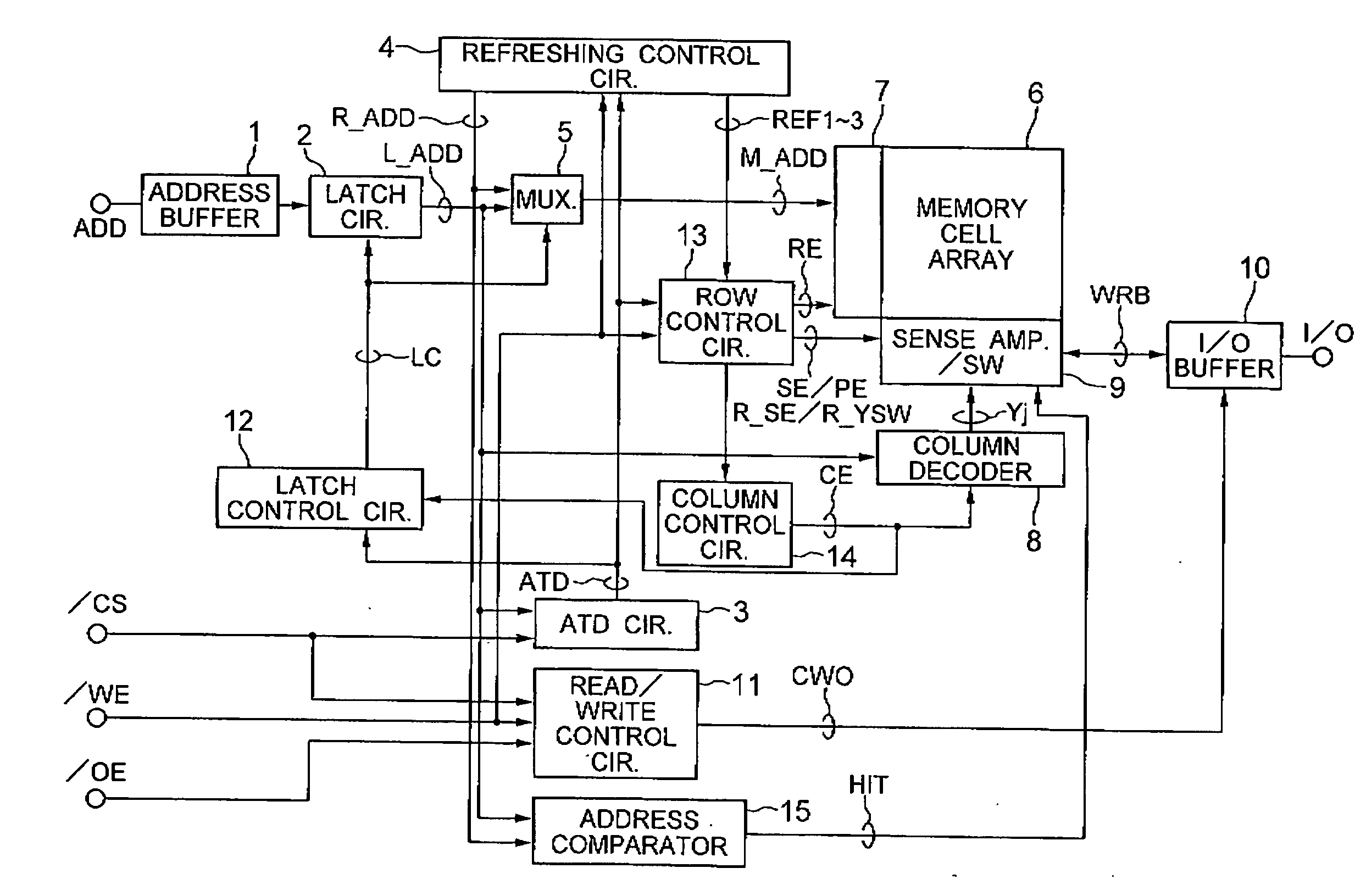
[0052] Referring to FIG. 1, there is shown a memory device according to the present invention. The memory device includes address buffer block 1, latch circuit 2, address transition detection (ATD) circuit 3, refreshing control circuit 4, multiplexer circuit 5, latch control circuit 12, read / write control circuit 11, address comparator circuit 15, row control circuit 13, column control circuit 14, row decoder 7, column decoder 8, sense amplifier / switch circuit 9, memory cell array 6 and I / O buffer block 10.

[0053] Symbol ADD represents an input address supplied from outside the memory device. The address buffer circuit 1 receives the input address ADD to deliver the same to the latch circuit 2, which delivers the input address ADD supplied from the address buffer circuit 1 as a latched address L_ADD if a latch control signal LC assumes a low level. If the latch control signal LC assumes a high level, the latch circuit 2 holds the latched address L_ADD latched at the rising edge of th...

second embodiment

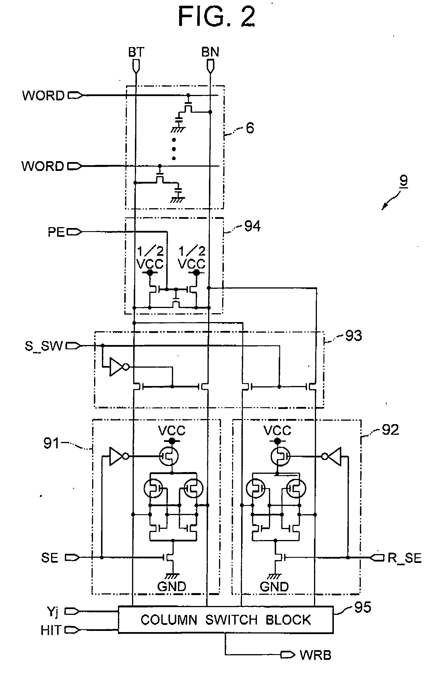
[0113] Referring to FIG. 10, there is shown a sense amplifier / switch circuit in a memory device according to the present invention. FIG. 11 shows the row control circuit shown in FIG. 10.

[0114] The sense amplifier / switch circuit 9A of FIG. 10 is roughly similar to the sense amplifier / switch circuit 9 of FIG. 2 except that the refreshing sense amplifier 92 in FIG. 2 is replaced by a SRAM-type data memory 97 having a SRAM memory cell structure in FIG. 10 and that NAND gates 911 to 913 are provided in the sense amplifier / switch circuit 9A in FIG. 10.

[0115] More specifically, the sense amplifier / switch circuit of FIG. 10 includes sense amplifier circuit 96, SRAM-type data memory 97, switch block 98, precharge circuit 99, column switch circuit 910, and NAND gates 911 to 913.

[0116] The sense amplifier circuit 96 is used both for the read / write operation for the input address ADD and the refreshing operation. The switch block 98 couples the bit lines BT and BN to respective sense amplifier...


PUM


Abstract

A semiconductor memory device includes a memory cell array including a plurality of memory cells having a DRAM cell structure and is treated as a SRAM memory device without controlling the data refreshing cycle for the memory cells. The refreshing cycle is separated into a read operation and a write operation, which sandwich therebetween a read/write operation for the input address of the memory cell. The data read in the refreshing cycle is saved in a refreshing sense amplifier during the read/write operation and stored in the memory cell after the read/write operation.

Description

[0001] (a) Field of the Invention[0002] The present invention relates to a semiconductor memory device having a DRAM (dynamic random access memory) cell structure and handled as a SRAM (static random access memory).[0003] (b) Description of the Related Art[0004] Semiconductor memory devices which have a DRAM cell structure and operating as SRAMs in the specification as viewed from the outside now play an important role in improving the functions of cellular phones which have been developed rapidly in these days. The advantages of this type of semiconductor memory device (may be referred to as simply "memory device" hereinafter) are that a periodic refreshing control from outside the memory device for maintaining the data stored in the memory cells, as encountered in the DRAM, is not needed to thereby allow easy handling thereof, and that the memory device has a larger capacity compared to the SRAM due to the simple DRAM cell structure.[0005] It is to be noted that the memory device ...

Claims


Application Information

Patent Timeline
Patent Type & Authority Applications(United States)
IPC IPC(8): G11C11/406G11C11/403G11C11/409H01L27/11
CPCG11C11/406G11C11/40615G11C11/40607H10B10/00
Inventor KAWAGUCHI, YASUNARI
Owner NEC ELECTRONICS CORP
Why Eureka
Try Eureka