Pulse output circuit, shift register and electronic equipment

a shift register and output circuit technology, applied in the direction of pulse technique, generating/distributing signals, instruments, etc., can solve the problems of difficult to reduce production cost, increase the number of steps, and increase the probability of malfunction of tft 205

Active Publication Date: 2004-07-22
SEMICON ENERGY LAB CO LTD
View PDF9 Cites 141 Cited by
  • Summary
  • Abstract
  • Description
  • Claims
  • Application Information

AI Technical Summary

Benefits of technology

[0154] According to the invention, a capacitance formed of first and second films each comprising either one of an active layer material, a gate electrode material and a wiring material, and of an insulating film provided between the first and second films may be used as the capacitance means.

Problems solved by technology

However, as for the manufacturing step of the CMOS circuit, the number of steps is increased due to the complicated steps of ion doping or the like, and thus, it is difficult to reduce the production cost.
However, the TFT 205 is likely to malfunction in the case of adopting a low voltage operation to reduce power consumption or the like.

Method used


Image

  • Pulse output circuit, shift register and electronic equipment
  • Pulse output circuit, shift register and electronic equipment
  • Pulse output circuit, shift register and electronic equipment

Examples


embodiment 1

[0176] FIGS. 3A and 3B show an example of the shift register described in the embodiment mode, which is additionally provided with a scanning direction switch function. In FIG. 3A, input terminals of scanning direction switch signal LR and of scanning direction switch back signal L / Rb are added to the shift register shown in FIG. 1A.

[0177] FIG. 3B shows a configuration of one stage of a pulse output circuit 300 in FIG. 3A. A main body of the pulse output circuit has the same configuration as that of FIG. 1B shown in the embodiment mode, while a scanning direction switch circuit 330 is additionally provided between the input signal terminals 2 and 3 and the main body of the pulse output circuit. The scanning direction switch circuit 330 includes TFTs 311 to 314.

[0178] As shown in FIG. 3B, gate electrodes of the TFTs 301 and 304 are connected to the input terminal 2 via the TFT 311 and to the input terminal 3 via the TFT 312. A gate electrode of the TFT 303 is connected to the input t...

embodiment 2

[0184] Explanation will be made on an example of the shift register described in the embodiment mode, which is additionally provided with an initialization signal (INI) as shown in FIG. 4A.

[0185] As shown in FIG. 4B, an initialization signal (INI) is inputted to a gate electrode of a TFT 411 added herein. When the TFT 411 is turned ON, a potential of a gate electrode of a TFT 406 is raised and the TFT 406 is turned ON, and thus, a potential of an output node is fixed at VSS.

[0186] Potentials of the output nodes can be fixed as VSS at all the stages by performing such initialization before the circuit starts to output a sampling pulse, that is, just after the power source is turned on, or during a fly-back period 460 provided in a part of a line period 450 as shown in FIG. 4C. In the case of employing a dynamic circuit as shown in the invention (circuit in which at least one node is in a floating state while operating), such initialization of the node or the like is effective for rea...

embodiment 3

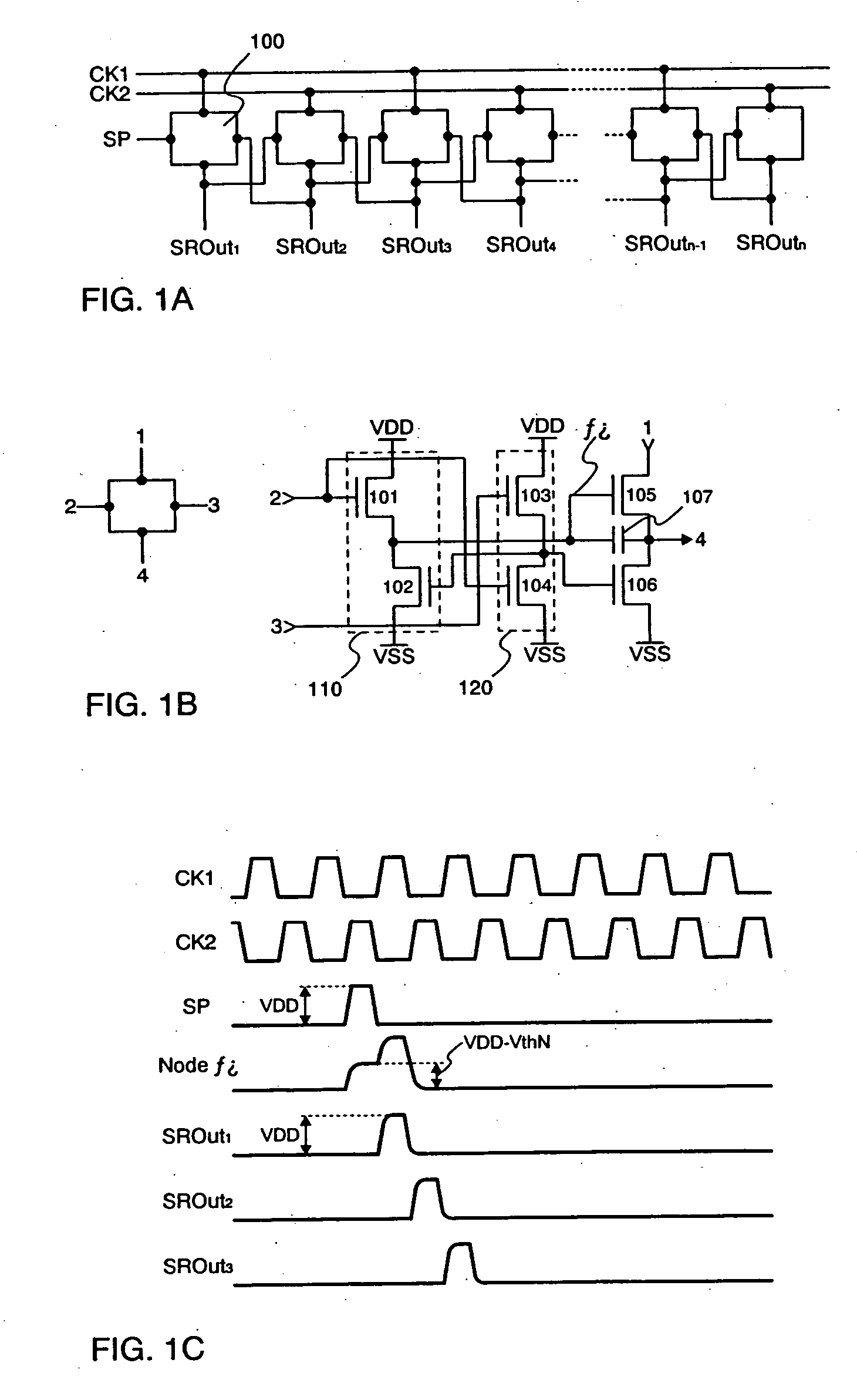
[0187] Focused here are states of the TFTs 101, 102, 105, and 106 during a period in which the pulse output circuit described in the embodiment mode operates (see FIG. 6A).

[0188] FIG. 6B shows a state of each node when a pulse is outputted from the (k-1)th stage of the pulse output circuit and subsequently, a pulse is outputted from the kth stage of the pulse output circuit. Focused here is a period in which a bootstrap operation is conducted in accordance with a rising potential of an output node (SROutk) during a period enclosed by a dotted line frame 601, namely at the kth stage.

[0189] As explained in the embodiment mode, the TFT 101 is turned ON and the potential of the node .alpha. is raised to (VDD-VthN) when a pulse at the preceding stage (the (k-1)th stage here) is outputted and inputted to the input terminal 2 at the kth stage (see FIG. 6C). In such a state, the voltage between the gate and source of the TFT 101 becomes lower than the threshold voltage, thereby turning OFF ...


PUM

PropertyMeasurementUnit
conductivityaaaaaaaaaa
electricallyaaaaaaaaaa
capacitanceaaaaaaaaaa

Abstract

A driver circuit of a display device, which includes TFTs of a single conductivity type and outputs an output signal with normal amplitude. A pulse is inputted to TFTs 101 and 104 to turn ON the TFTs and a potential of a node alpha is raised. When the potential of the node alpha reaches (VDD-VthN), the node alpha becomes in a floating state. Accordingly, a TFT 105 is turned ON and a potential of an output node is raised as a clock signal becomes High level. On the other hand, a potential of a gate electrode of the TFT 105 is further raised due to an operation of a capacitance means 107 as the potential of the output node is raised, so that the potential of the gate electrode of the TFT 105 becomes higher than (VDD+VthN). Thus, the potential of the output node is raised to VDD without causing a voltage drop due to a threshold voltage of the TFT 105. An output at the subsequent stage is then inputted to a TFT 103 to turn the TFT 103 ON, while the potential of the node alpha of TFTs 102 and 106 is dropped to turn the TFT 105 OFF. As a result, the potential of the output node becomes Low level.

Description

[0001] 1. Field of the Invention[0002] The present invention relates to a pulse output circuit, a shift register and a display device.[0003] 2. Description of the Related Art[0004] In recent years, a display device in which a circuit is formed on an insulating substrate, specifically on a glass or plastic substrate, by using thin film transistors (hereinafter referred to as TFTs) formed of a semiconductor thin film has been developed. Specifically, development of an active matrix display device has been remarkably advanced. The active matrix display device formed of TFTs includes hundred thousands to millions of pixels which are arranged in matrix, and the TFTs provided in each pixel control the charge of each pixel to display an image.[0005] Further, polysilicon TFTs which have excellence in electrical properties have been developed instead of amorphous TFTs. By using the polysilicon TFTs, a method of forming a driver circuit in the periphery of a pixel portion simultaneously with ...

Claims


Application Information

Patent Timeline
Patent Type & Authority Applications(United States)
IPC IPC(8): G02F1/133G02F1/1345G02F1/1368G06F1/04G09G3/20G09G3/36G11C19/00G11C19/28H01L51/50H03K3/013H03K3/353H03K17/00H03K17/693H03K19/0175H03L5/00H05B33/14
CPCG09G3/3688G11C19/28G11C19/00G09G2310/0275E05B65/025E05B65/44
Inventor NAGAO, SHOUTANADA, YOSHIFUMISHIONOIRI, YUTAKAMIYAKE, HIROYUKI
Owner SEMICON ENERGY LAB CO LTD
Why Eureka
Try Eureka