Ball grid array package construction with raised solder ball pads

a grid array and solder ball technology, applied in the direction of printed circuit non-printed electric components association, sustainable manufacturing/processing, final product manufacturing, etc., can solve the problems of adding cost to the package, unable to achieve the clearance required using a typical bga solder ball, and incompatible with desired board-level assembly processes

Inactive Publication Date: 2004-07-22
ULTRATECH INT INC
View PDF77 Cites 11 Cited by
  • Summary
  • Abstract
  • Description
  • Claims
  • Application Information

AI Technical Summary

Problems solved by technology

Attachment of the chip on the underside of the interposer can pose a clearance difficulty.
If it is desired to have an approximately 200 micron clearance between the chip and the bottom substrate of the package, it would be difficult or impossible to achieve the necessary clearance using a typical BGA solder ball array having solder balls in the range of 400 to 600 microns in diameter connected to the bottom of a circuit substrate, without thinning the inactive face of the chip.
Although solder columns could be used to provide the necessary clearance for a chip mounted on the underside of the package as described above, this would add cost to the package and additionally may not be compatible with desired board-level assembly processes.

Method used


Image

  • Ball grid array package construction with raised solder ball pads
  • Ball grid array package construction with raised solder ball pads
  • Ball grid array package construction with raised solder ball pads

Examples


Embodiment Construction

[0060] The foregoing and other objects, features and advantages of the invention will be apparent from the following more particular description of a preferred embodiment of the invention, as illustrated in the accompanying drawings, wherein like reference numbers represent like parts.

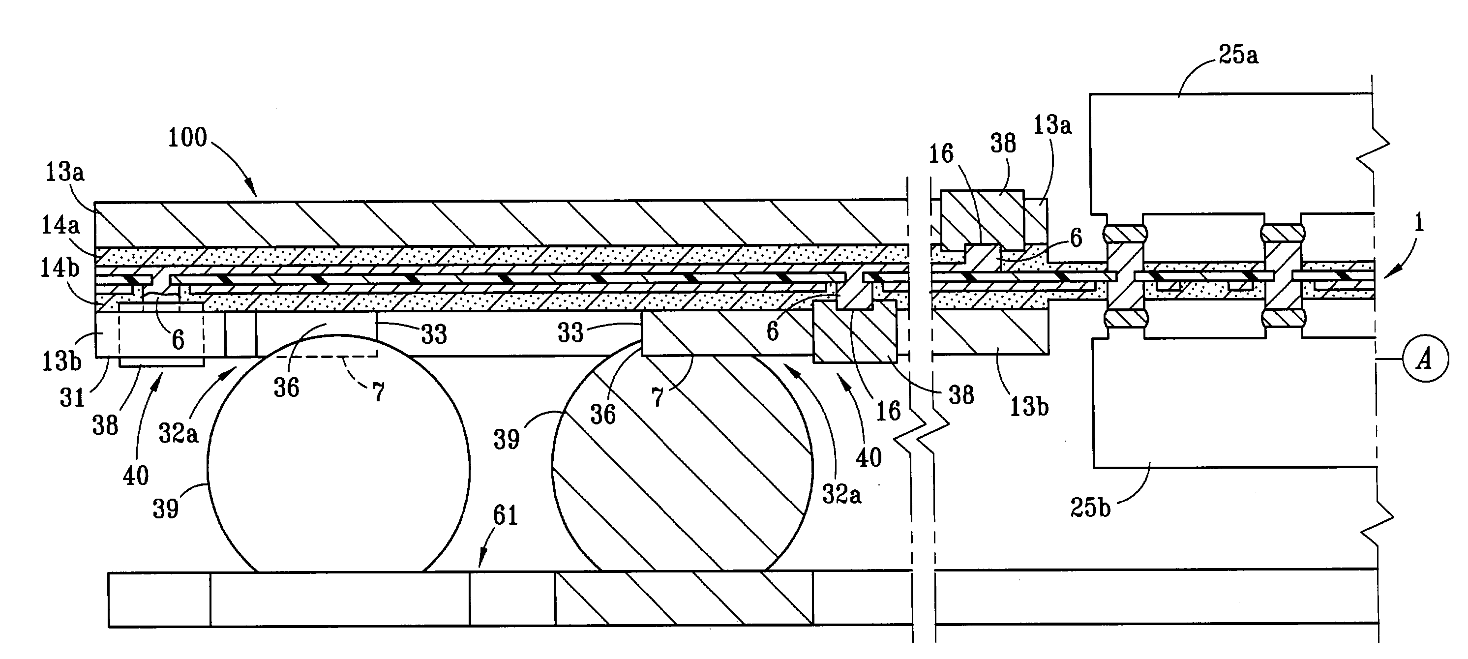
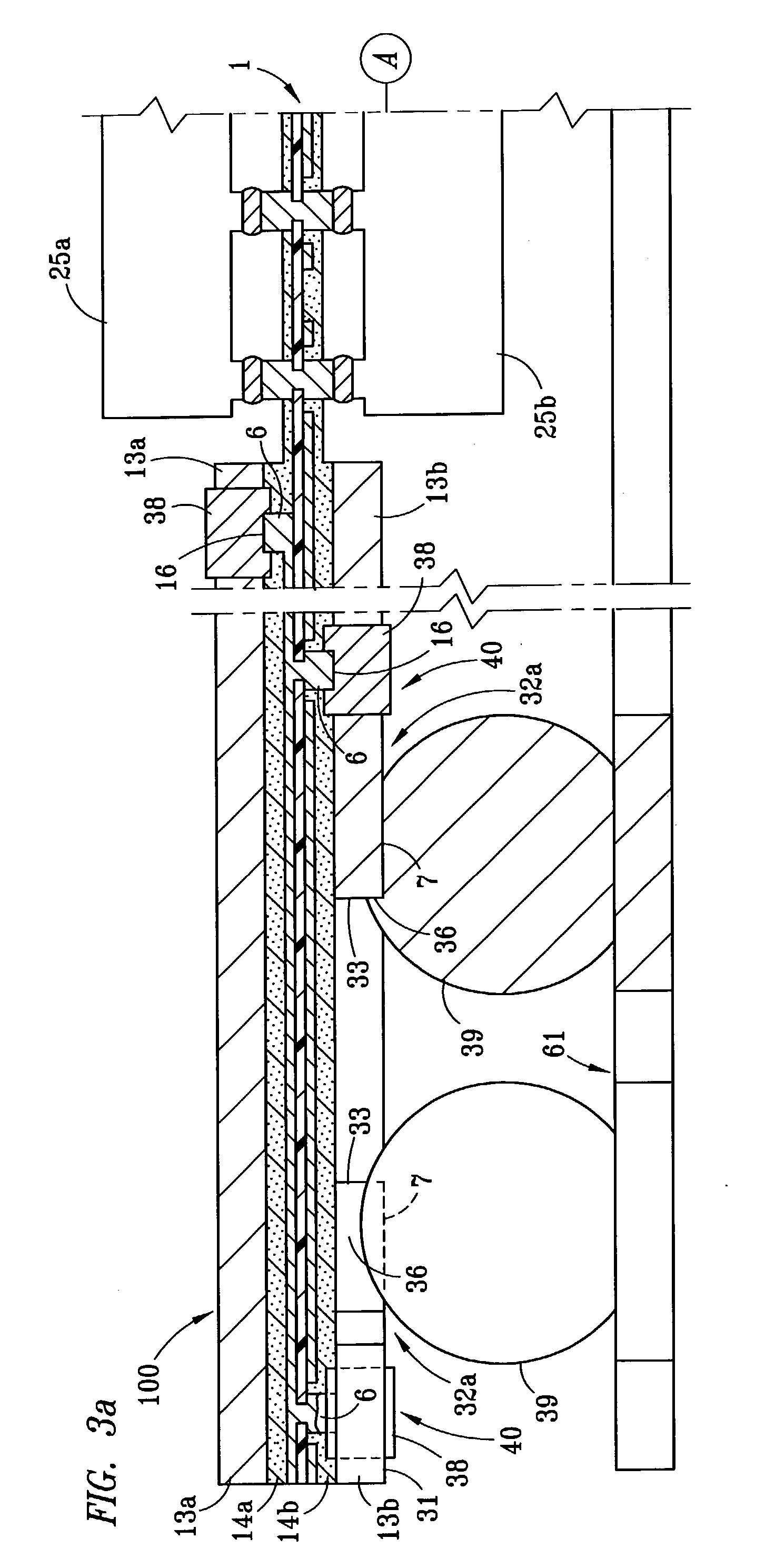
[0061] Referring now to the drawings in detail, and initially to FIG. 5 thereof, a crosssectional view of a typical prior art interconnection between a BGA solder ball 39 and its connection pad 55 on a trace 56 of a circuit substrate 57 is depicted. Taking into account that the solder ball is flattened somewhat where it connects to the substrate, if a 600 micron solder ball is used, the distance "a" between the lower face of the circuit layer (not counting the solder mask layer) and the bottom of the solder ball will be about 500 microns from the connection pad 55.

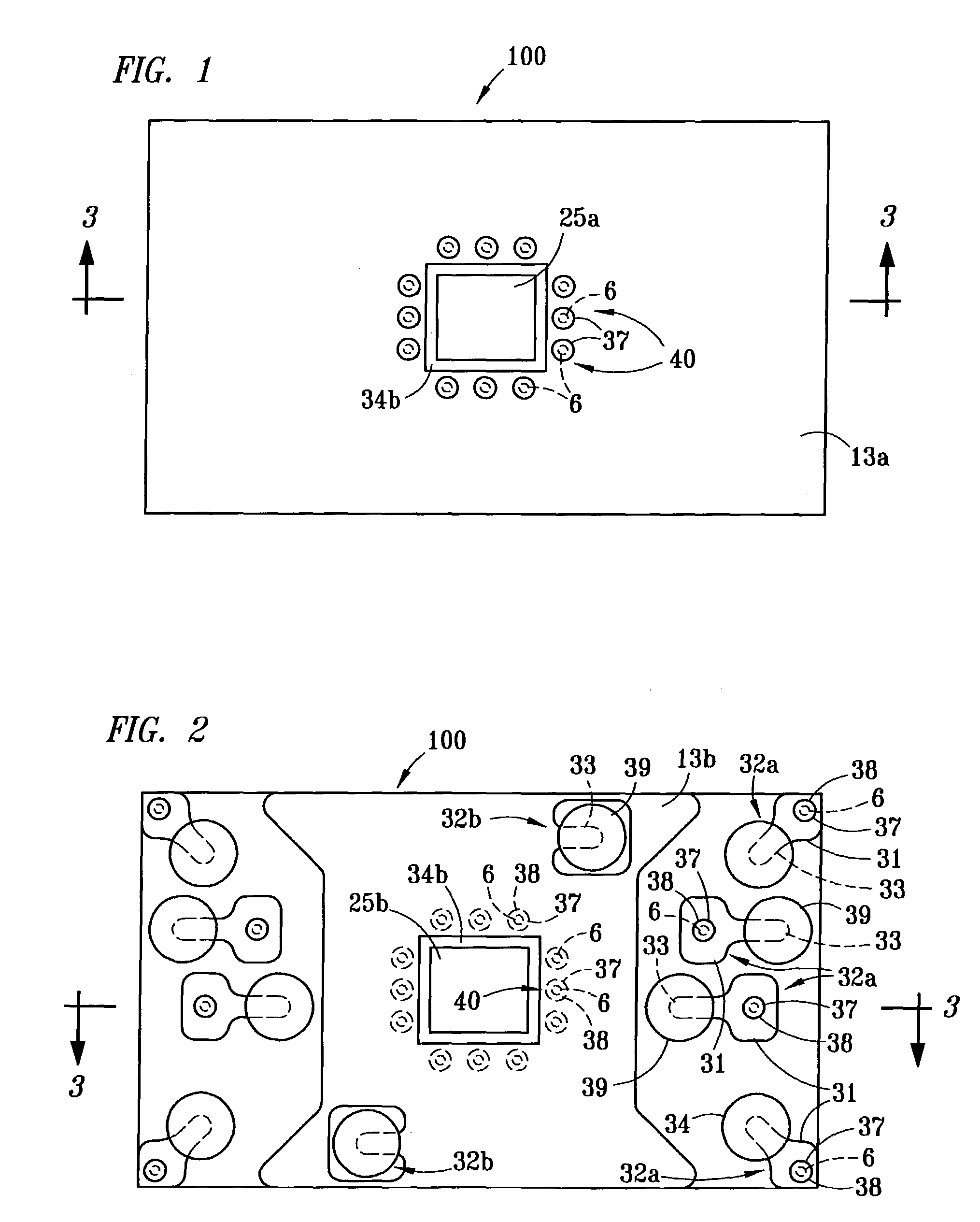
[0062] Referring now to FIG. 2, a raised pad 32a for a BGA solder ball 39 in accordance with the present invention is depicted. The raised s...


PUM


Abstract

The present invention provides for a BGA solder ball interconnection to an outer conductive layer of a laminated circuit assembly having an underlying circuit layer. The invention includes a raised BGA solder ball pad substantially co-planar with the outer conductive layer, the raised pad having a raised face and a plurality of vertical conductive walls and a BGA solder ball having an average diameter of greater than the width of the raised face, the BGA solder ball being adhered to the raised face and to a substantial portion of the vertical conductive walls.

Description

CROSS-REFERENCED APPLICATIONS[0001] This application relates to co-pending U.S. patent applications entitled "Method and Apparatus for Interconnecting a Relatively Fine Pitch Circuit Layer and Adjacent Power Plane(s) in a Laminated Construction" (Docket No. AUS920020578US1) and "Flex-Based IC Package Construction Employing a Balanced Lamination" (Docket No. AUS920020579US1), filed concurrently herewith, the contents of which are hereby incorporated by reference.BACKGROUND OF THE INVENTION[0002] 1. Field of the Invention[0003] This invention relates generally to the field of integrated circuit packaging.[0004] 2. Description of the Related Art[0005] In the manufacture of integrated circuits, extremely fine circuits are photolithographically placed onto a chip, also called a die. The circuits on the chip terminate at conductive terminals on the face of the chip, which must be electrically connected to power and to other chips. For protection of the chip and ease of handling, the chips...

Claims


Application Information

Patent Timeline
Patent Type & Authority Applications(United States)
IPC IPC(8): H01L23/498H01L25/065H01L23/12H01L25/07H01L25/18H05K1/11H05K3/34H05K3/46
CPCH01L23/49816H01L25/0657H01L2924/00014H01L2224/16225H05K1/111H05K3/3436H05K3/3452H05K3/3457H05K3/4652H05K2201/098H05K2201/0989Y02P70/611H01L2225/06589H01L2225/06513H01L2225/06572H01L2224/0401Y02P70/50
Inventor HARVEY, PAUL MARLAN
Owner ULTRATECH INT INC
Why Eureka
Try Eureka