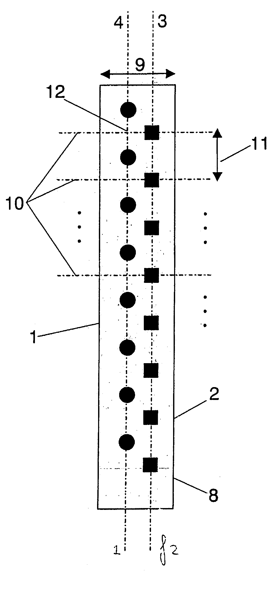
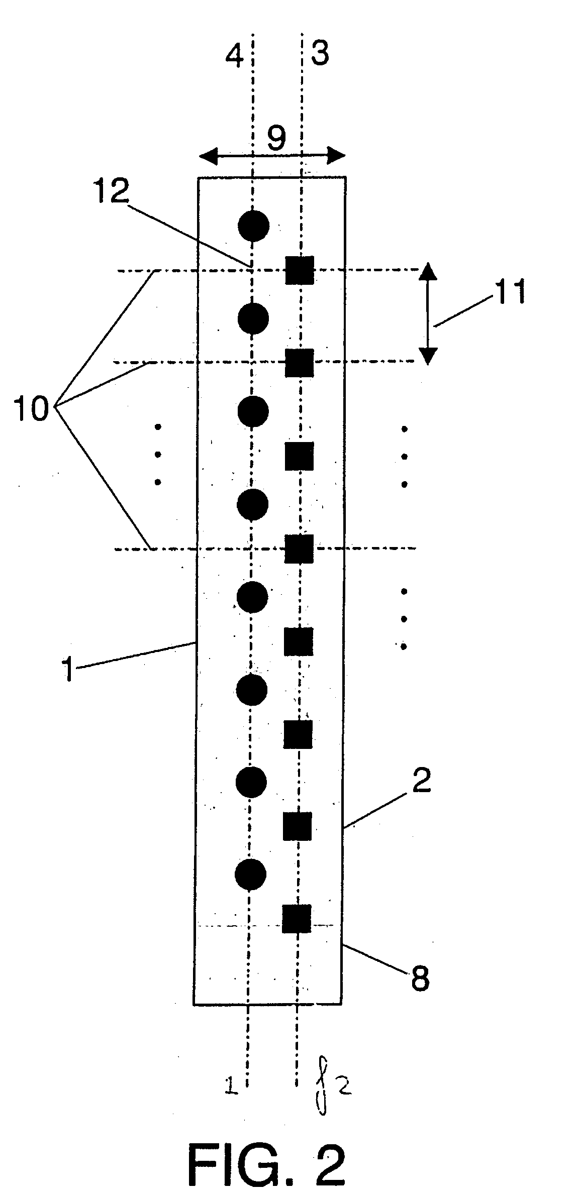
[0020] An scheme of the basic layout for the spatial arranging (interleaving) of the antenna elements is shown in FIG. 2. The solid dots (1) display the positions of the elements for the lower frequency f1, while the squares (2) display the positions for the antenna elements for the upper frequency f2. Antenna elements for the higher frequency band f2 are aligned along a vertical axis (3) with the desired spacing between elements (11). Said spacing is slightly smaller than a full-wavelength (typically below 98% the size of the shorter wavelength) for a maximum gain, although it can be readily seen that the spacing can be made shorter depending on the application. A second vertical column of elements for the lower frequency band f1 is aligned along a second vertical axis (4) placed next to said first axis (3) and substantially parallel to it. In the particular arrangement of FIG. 2 low-frequency elements are placed along the left axis (4) while high-frequency elements are place along the right axis (3), but obviously the position of both axes could be exchanged such that low-frequency elements would be place on the right side and vice versa. In any case, the spacing (9) between said axis (3) and (4) is chosen to fall between 0.1 and 1.2 times the longer wavelength.
[0021] The shorter wavelength (corresponding to f2) determines the spacing between elements (11) at both axis. Usually a spacing below a 98% of said shorter wavelength is preferred to maximize gain while preventing the introduction of grating lobes in the upper band; this is possible due to the spacing between frequency bands which is always f2/f1<1.5 according to the present invention. Regarding the relative position of elements (1) and (2), elements for f2 are placed at positions (2) along vertical axis (3) and horizontal axes (10) such that the horizontal axes (10) intersect both with the positions of said elements (2) and the mid-point (12) between elements (1) at the neighbor axis (4); this ensures a maximum distance between elements and therefore a minimum coupling between elements of different bands.
[0022] Having independent elements for each band, the array is easily fed by means of two-separate distribution networks. Corporate feed or taper networks in microstrip, strip-line, coaxial or any other conventional microwave network architecture described in the prior art can be used and do not constitute an characterizing part of the invention. It is interesting however to point out that by using independent networks an independent phasing of the elements at each band can be used within the present invention, which is in turn useful for introducing either a fix or adjustable electrical down-tilt of the radiation pattern at each band independently.
[0023] Optionally and depending on the particular set of frequencies of f1 and f2, it is clear to those skilled in the art that any other dual-band or broad-band feeding network described in the prior art can be also used within the spirit of the present invention.
[0024] Regarding the antenna elements, any dual-polarized antenna elements (for instance crossed dipole elements, patch elements) can be used according to the scope of the present invention, however a radiating element of reduced size is preferred to reduce the coupling between them. A small dual-polarized patch element with a space-filling perimeter is proposed here as a particular example for a possible array implementation (FIG. 3). For the same purpose, other dual-polarized space-filling miniature antenna elements, such as for instance those described in patent PCT/EP00/00411, can be used as well.
[0025] The same basic configuration of dual-band array described here features different beam widths and shapes in the horizontal plane depending on the spacing between elements in the horizontal direction. For this purpose, several elements within the array can be placed at a shifted horizontal position with respect to either axis (3) or (4) according to the present invention. Typically, the shift with respect to said axis (3) or (4) is smaller than 70% of the longer operating wavelength. A particular case of such a displacement consists on tilting a few degrees (always below 45.degree.) one or both of said reference axis such that the displacement is uniformly increased either upwards or downwards. FIG. 4 shows as an example a particular embodiment where the some elements are displaced from the axis, while FIG. 5 shows another embodiment where the axis (3) and (4) are slightly tilted. As it would be obvious to those skilled in the art, other shifting and tilting schemes can be used for the same purpose within the scope of the present invention.
[0026] As it can be readily seen by anyone skilled in the art, the number of elements and the vertical extent of the array is not a substantial part of the invention; any number of elements can be chosen depending on the desired gain and directivity of the array. Also, the number of elements and vertical extent of the array does not need to be the same; any combination in the number of elements or vertical extent for each band can be optionally chosen within the spirit of the present invention.
[0027] Beyond the specific coordinate position of the elements, the skilled person will notice that any rotation of the elements to for instance obtain other kind of polarizations states or changes in the antenna parameters as described in the prior art can be also applied to the present invention.
[0028] A preferred embodiment of the present invention is an array that operates simultaneously at the GSM1800 (1710-1880 MHz) and UMTS (1900-2170 MHz) frequency bands. The antenna features .+-.45.degree. dual-polarization at both bands and finds major application in cellular base stations (BTS) where both services are to be combined into a single site. The basic configuration of a particular embodiment for such a configuration is shown in FIG. 6.
[0029] The antenna is designed with 8 elements operating at GSM1800 (13) and 8 elements operating at UMTS (14) to provide a directivity above 17 dBi. The elements are aligned along two different axes (3) and (4), one for each band. According to the present invention, elements (13) for GSM1800 are interleaved in the vertical direction with respect to elements for UMTS (14) to reduce the coupling between elements by maximizing the distance between them, yet keeping a minimum distance between said axes (3) and (4). For this particular embodiment, the spacing between axes (3) and (4) must be larger than 40 mm if an isolation between input ports above 30 dB (as usual for cellular systems) is desired.
[0030] Depending on the required gain, it is clear to anyone skilled in the art that the number of elements can be enlarged or reduced beyond 8. The number of elements can be even different for each band to achieve different gains. To operate at this particular bands, the vertical spacing between elements must be chosen to fall within the range of 100 mm to 165 mm. For an 8-element array and a gain around 17 dBi the elements are mounted upon a substantially rectangular ground-plane (8) with an overall height within a range of 1100 mm up to 1500 mm.
[0031] Any kind dual-polarized single-band radiating elements can be used for this antenna array within the scope of the present invention, such as for instance crossed dipoles or circular, squared or octagonal patches, however innovative space-filling patches such as those in drawings (13) and (14) are preferred here because they feature a smaller size (height, width, area) compared to other prior art geometries. Said space-filling patches can be manufactured using any kind of the well-known conventional techniques for microstrip patch antennas and for instance can be printed over, a dielectric substrate such as epoxy glass-fiber (FR4) substrates or other specialized microwave substrates such as CuClade.RTM., Arlon.RTM. or Rogers.RTM. to name a few. Said elements are mounted parallel to a conducting ground-plane (8) and typically supported with a dielectric spacer. It is precisely the combination of the particular spatial arrangement of the elements (vertical interleaving and proximity of vertical axis) together with the reduced size and the space-filling shape of the patch antenna elements that the whole antenna size is reduced. The size of the antenna is basically the size of the ground-plane (8) which for this particular embodiment must be wider than 140 mm but it can be typically stretched below 200 mm, which is a major advantage for a minimum visual environmental impact on landscapes compared to other conventional solutions such as the one described in FIG. 1
[0032] The elements can be fed at the two orthogonal polarization feeding points located at the center of the circles (15) by means of several of the prior-art techniques for patch antennas, such as for instance a coaxial probe, a microstrip line under the patch or a slot on the ground-plane (8) coupled with a distribution network beyond said ground-plane. For a dual-band dual-polarization operation four independent feeding and distribution networks (one for each band and polarization) can be used. According to the preferred embodiment, said feeding networks are mounted on the back-side of the ground-plane and any of the well-known configurations for array networks such as for instance microstrip, coaxial or strip-line networks can be used since does not constitute an essential part of the invention.
[0033] Regarding the relative position of the feeding points (15) upon the patch, FIG. 6 shows an embodiment where said feeding points are located at the inner side towards the center of the ground-plane, that is, at the right side of axis (4) for the lower band and at the left side of axis (3). Those skilled in the art will notice that any other embodiments can be used as well within the scope of the present invention, such as for instance: all elements with feeding points at the left part of their respective axes, all feeding points on the right side, some elements on the right side and some on the left side, or even some elements with a feeding point at each side of the corresponding axis is possible within the scope of the present invention.
[0034] In the preferred embodiment, the overall antenna array with the elements, ground-plane and feeding network is mounted upon a conventional shielding metallic housing enclosing the back part of the ground-plane, said housing also acting for a support of the whole antenna. Also, a conventional dielectric radome covering the radiating elements and protecting the whole antenna from weather conditions is also mounted and fixed to the housing as in any conventional base-station antenna.
[0035] The antenna would naturally include 4 connectors (typically {fraction (7/16)} connectors), one for each band and polarization, mounted at the bottom part of the ground-plane. Each connector is then been connected through a transmission line (such as for instance a coaxial cable) to the input port of each feeding network.
[0036] The skilled in the art will notice that other connector combinations are possible within the scope of the present invention. For instance, a filter duplexer can be used to combine the input ports of the +45.degree. GSM1800 and UMTS networks into a single connector, and the 45.degree. GSM1800 and UMTS networks into another single connector to yield a total of only two connectors. Said duplexer can be any duplexer with a 30 dB isolation between ports and does not constitute an essential part of the present invention. Obviously, and alternative solution such as a broadband or dual-band network combining GSM1800 and UMTS for the +45.degree. and another one for the -45.degree.polarization could be used instead of the diplexer, which yields to a two-connector configuration as well.
[0037] Having illustrated and described the principles of our invention in several preferred embodiments thereof, it should be readily apparent to those skilled in the art that the invention can be modified in arrangement and detail without departing from such principles.