[0020] In the production method of a film carrier tape according to the invention, the film carrier tape is washed within 6 seconds after the film carrier tape exit the plating tank to remove the plating solution which remains on the surface of the film carrier tape. By controlling the time for which the film carrier tape is subjected to contact with the plating solution within 6 seconds after exiting the plating tank, a substitution may be substantially prevented from occurring between bismuth in the plating solution and tin in a tin-bismuth alloy deposit formed at lead portions of the film carrier tape.
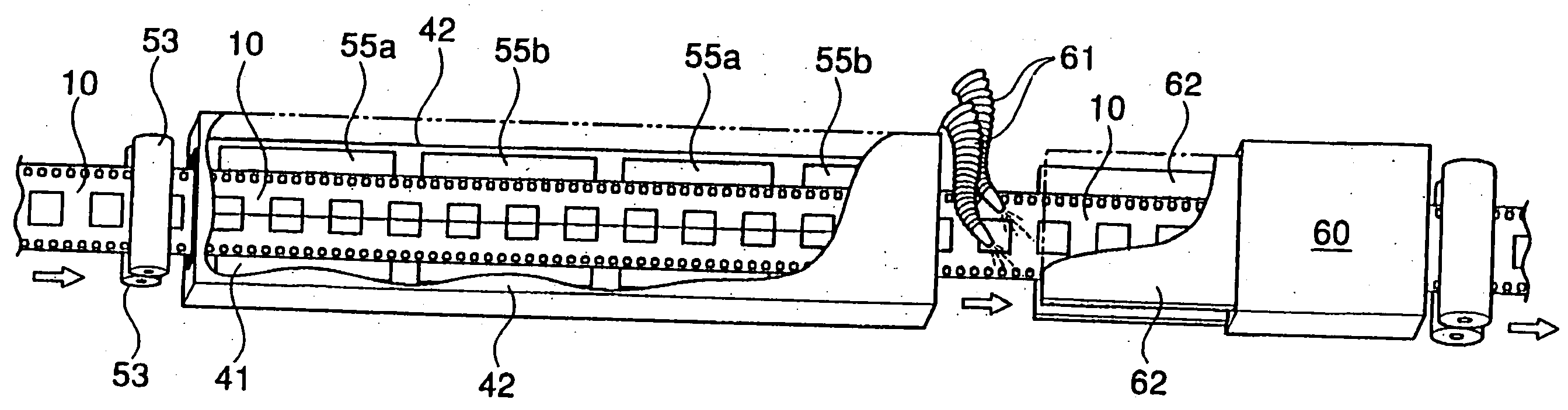
[0087] The plating apparatus according to the invention is provided with a washing
nozzle 61 which performs the washing of the film carrier tape 10 carried out from the plating tank 42 through the slit outlet opening 51 before the film carrier tape 10 reaches the washing tank 60. The washing nozzle 61 should be arranged to be able to wash off at least the plating solution remaining on the wiring pattern of the film carrier tape 10. At least two washing nozzles will be preferably provided to wash both surfaces of the film carrier tape 10 at the same time because the surface with the wiring pattern turns around depending on the standing condition of the film carrier tape 10 carried out through the slit outlet opening 51, and flowing of the plating solution to the back surface of the film carrier tape 10 through the holes formed in the tape, such as
sprocket holes or device holes, may possibly occur. The washing nozzles 61 are positioned so that the film carrier tape 10 can be washed within 6 seconds, preferably within 5 seconds, after the corresponding part of the film carrier tape exits the plating tank 42 through the slit outlet opening 51. Preferably, the washing nozzles 61 are directed to eject water toward the traveling direction of the film carrier tape 10. To allow for appropriate adjustment of the ejection point and the ejection angle of water with respect to the film carrier tape 10, each washing nozzle 61 is preferably provided in connection with a
bellows flexible tube. The washing nozzle may be arranged at the tip of the
bellows flexible tube. A feed rate of water from the washing nozzles 61 is suitably 10 to 500 ml / sec, and preferably 30 to 300 ml / sec. A
water pressure therefrom is suitably 0.05 to 0.8 kgf / cm.sup.2, and preferably 0.2 to 0.5 kgf / cm.sup.2. By adjusting the feed rate and the
water pressure within the above ranges, the plating solution remaining on the film carrier tape 10 may be effectively washed off without deforming the wiring pattern, particularly the connection leads.
[0088] To prevent the water ejected from the washing nozzles 61 from scattering, the plating apparatus 40 is preferably provided with receivers 62 which extend aside from both surfaces of the film carrier tape 10 in the parallel direction. Since the washing nozzles 61 eject washing water along the traveling direction of the film carrier tape 10, the receivers 62 will be provided at any downstream point of the traveling direction of the film carrier tape 10 past the washing nozzles 61. The receivers 62 can be arranged to connect the plating tank 42 with the washing tank 61. The width between the receivers 62 is nearly equal to or greater than the width of the film carrier tape 10 to be washed. By impinging on the receivers 62, it can be prevented that the water is scattered around, and the removal of the plating solution remaining on the film carrier tape 10 can be enhanced.
[0090] As described above, the film carrier tape 10 can be washed with the jet of washing water applied from the washing nozzles 61 within 6 seconds, preferably within 5 seconds, after the film carrier tape 10 exits the plating tank 42. Since the plating solution can be almost completely removed from the film carrier tape 10 in such a short period of time, the substitution between tin on the surface of the tin-bismuth alloy deposit 19 formed on the connection leads and bismuth in the plating solution remaining on the alloy deposit 19 can be effectively prevented. As a consequence, a bismuth content in the tin-bismuth alloy deposit formed on the lead portion of the film carrier tape will be substantially homogeneous along its thickness direction. That is, the composition of the tin-bismuth alloy is constant at any portion of the tin-bismuth alloy deposit. Therefore, the melting point of the tin-bismuth alloy will not fluctuate and stable bonding properties can be obtained all the time.
[0091] As such, the composition in the tin-bismuth alloy deposit 19 formed to the film carrier tape of the invention is constant. That is, the bismuth content in the vicinity of the surface of the tin-bismuth alloy deposit 19 is substantially the same with that deep inside thereof. Therefore, stable bonding properties can be obtained.

