Printed circuit board, method for producing same and semiconductor device
a technology of printed circuit boards and semiconductor devices, which is applied in the direction of transportation and packaging, association of printed circuit non-printed electric components, and metal adhesion improvement of insulating substrates, etc., can solve the problem of not being able to achieve the effect of increasing the surface area of opposing electrodes, and achieve the effect of increasing the surface area of electrodes
- Summary
- Abstract
- Description
- Claims
- Application Information
AI Technical Summary
Benefits of technology
Problems solved by technology
Method used
Image

Examples
first embodiment
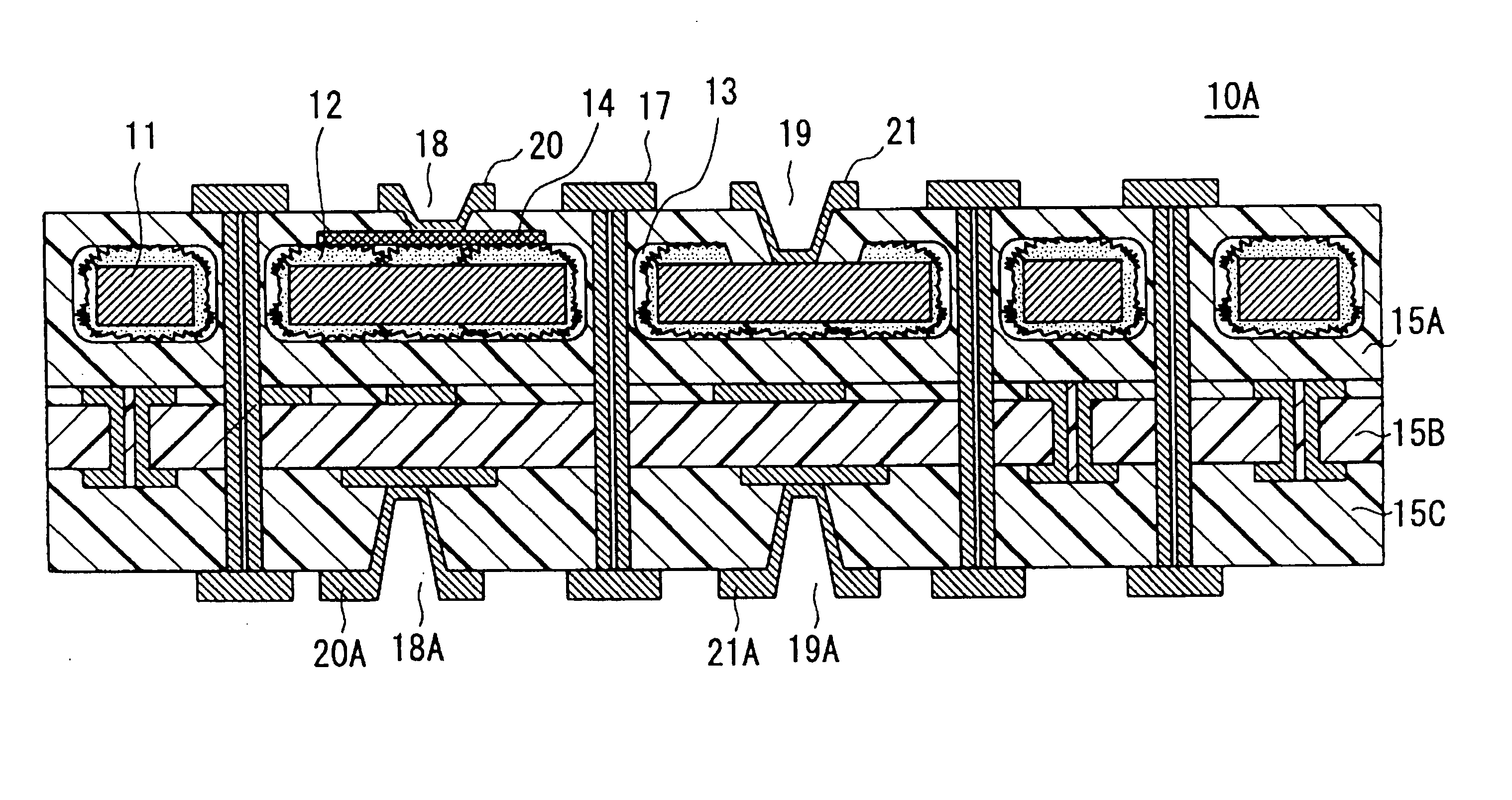
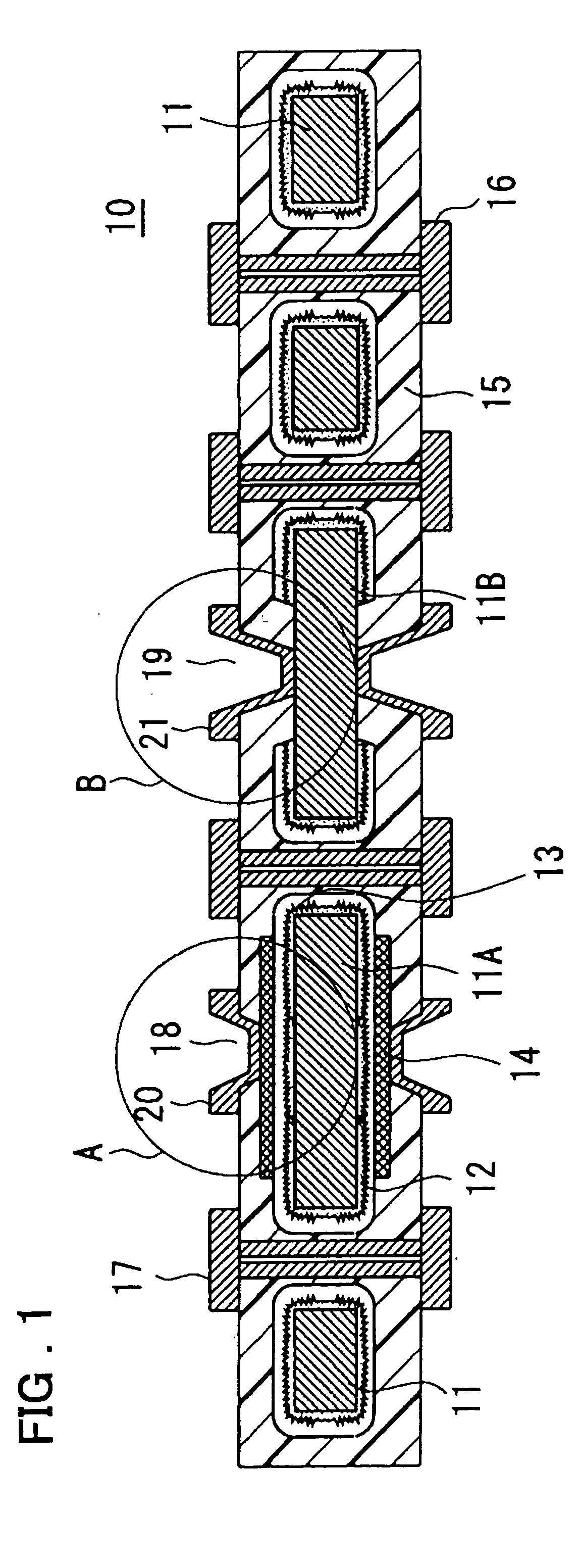
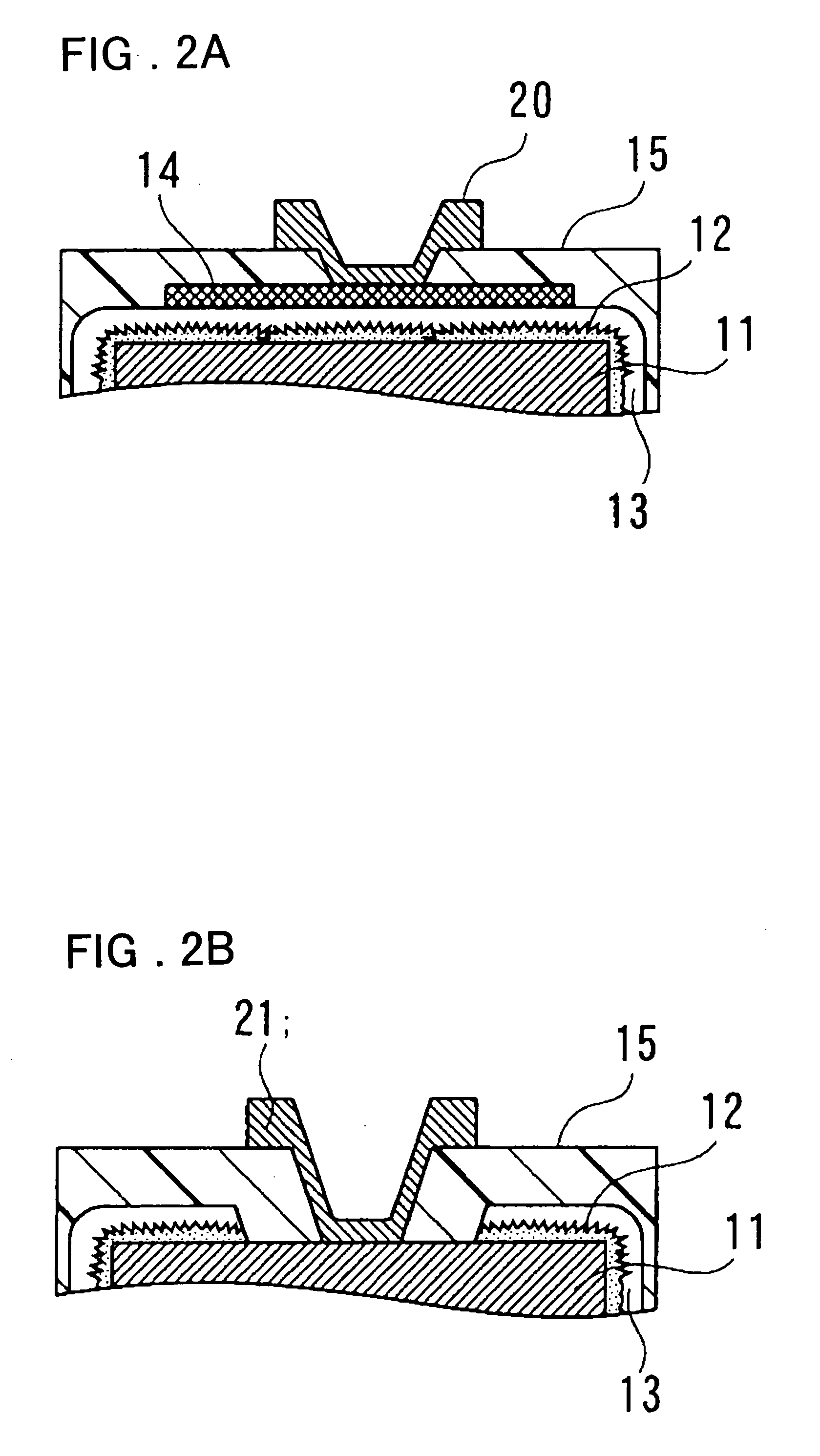
[0088] For more detailed description of the above-described embodiments of the present invention, the embodiments of the present invention are now explained with reference to the drawings. FIGS. 1 and 2 illustrate the structure of the present invention.
[0089] An aluminum sheet (Al sheet) 11, forming a metal core substrate of the printed circuit board, has a roughed surface. Specifically, micro-irregularities are formed on the surface of the foil-shaped aluminum sheet 11 by e.g., etching. By employing a metal sheet, e.g., aluminum sheet 11 as a core substrate, it is possible to reduce the substrate thickness and yet to provide for the required strength.
[0090] On the surface of the aluminum sheet 11, an aluminum oxide (Al oxide) layer 12, as a dielectric film for a capacitor, is formed to a thickness having e.g., hundreds of picometers (pm), where 1 pm is 10.sup.-12 m, as a lower limit and having e.g., tens of nanometers (nm) as an upper limit. The thin film of the aluminum oxide laye...
second embodiment
[0106] That is, in the second embodiment, the electrical insulation across the anode side electrode 21 and the layer of the electrically conductive high molecular material 13 is assured by the insulating resin 22.
[0107] As this insulating resin 22, an etching resist, operating as a mask for roughing processing of the aluminum sheet 11, may also be used, as will be explained later on in connection with the explanation of the manufacturing method. The etching resist in this case is left over unchanged on the aluminum sheet 11 after the roughing processing (the etching resist is termed a [permanent resist]).
[0108] Referring to FIGS. 3 and 4B, the area of the via for anode side connection on the surface of the aluminum sheet 11, and the near-by area where the insulating resin 22 is formed, are at a higher height level than the other peripheral area where there are provided the aluminum oxide layer 12 and the layer of the electrically conductive high molecular material 13, by way of prov...
third embodiment
[0114] Thus, in the present third embodiment of the present invention, the electrical insulation between the electrode 21 of the anode and the cathode side by the insulating resin 22 provided between the electrode 21 on one hand and the metal plating layer 23 and the layer of the electrically conductive high molecular material 13 on the other hand is assured. That is, the electrical insulation between the anode electrode 21 on one hand and the metal plating layer 23 and the layer of the electrically conductive high molecular material 13 on the other hand is assured by the insulating resin 22.
[0115] As this insulating resin 22, an etching resist, operating as a mask for roughing processing of the aluminum sheet 11, may also be used, as will be explained later on in connection with the explanation of the manufacturing method. The etching resist in this case is left over unchanged on the aluminum sheet 11 after the roughing processing.
[0116] The area of the via for anode side connectio...
PUM
| Property | Measurement | Unit |
|---|---|---|
| thickness | aaaaa | aaaaa |
| thickness | aaaaa | aaaaa |
| thickness | aaaaa | aaaaa |
Abstract
Description
Claims
Application Information