SRAM cell design with high resistor CMOS gate structure for soft error rate improvement

a technology of cmos gate structure and resistor, which is applied in the direction of digital storage, semiconductor/solid-state device details, instruments, etc., can solve the problems of soft errors, particle-induced soft errors, and the state of the memory cell to change,

Inactive Publication Date: 2004-12-16
TAIWAN SEMICON MFG CO LTD
View PDF22 Cites 40 Cited by
  • Summary
  • Abstract
  • Description
  • Claims
  • Application Information

AI Technical Summary

Problems solved by technology

Reduced, sub-micron level geometries and reduced operating voltages deployed in these chips make them vulnerable to particle induced soft errors.
Typically, soft errors occur when charged particles penetrate a memory cell and cross a junction, creating an abnormal charge that undesirably causes the state of the memory cell to change.
Among the common sources of soft errors are alpha ...

Method used


Image

  • SRAM cell design with high resistor CMOS gate structure for soft error rate improvement
  • SRAM cell design with high resistor CMOS gate structure for soft error rate improvement
  • SRAM cell design with high resistor CMOS gate structure for soft error rate improvement

Examples


Embodiment Construction

[0021] While the invention is susceptible to various modifications and alternative forms, specific embodiments thereof are shown by way of example in the drawings and will be described herein in detail. It should be understood, however, that the drawings and detailed description thereto are not intended to limit the invention to the particular form disclosed, but on the contrary, the intention is to cover all modifications, equivalents and alternatives falling within the spirit and scope of the present invention as defined by the appended claims.

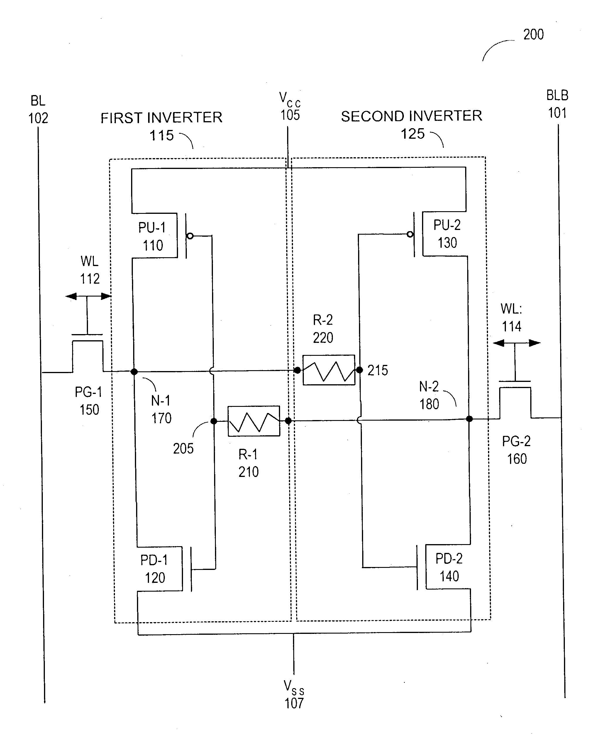
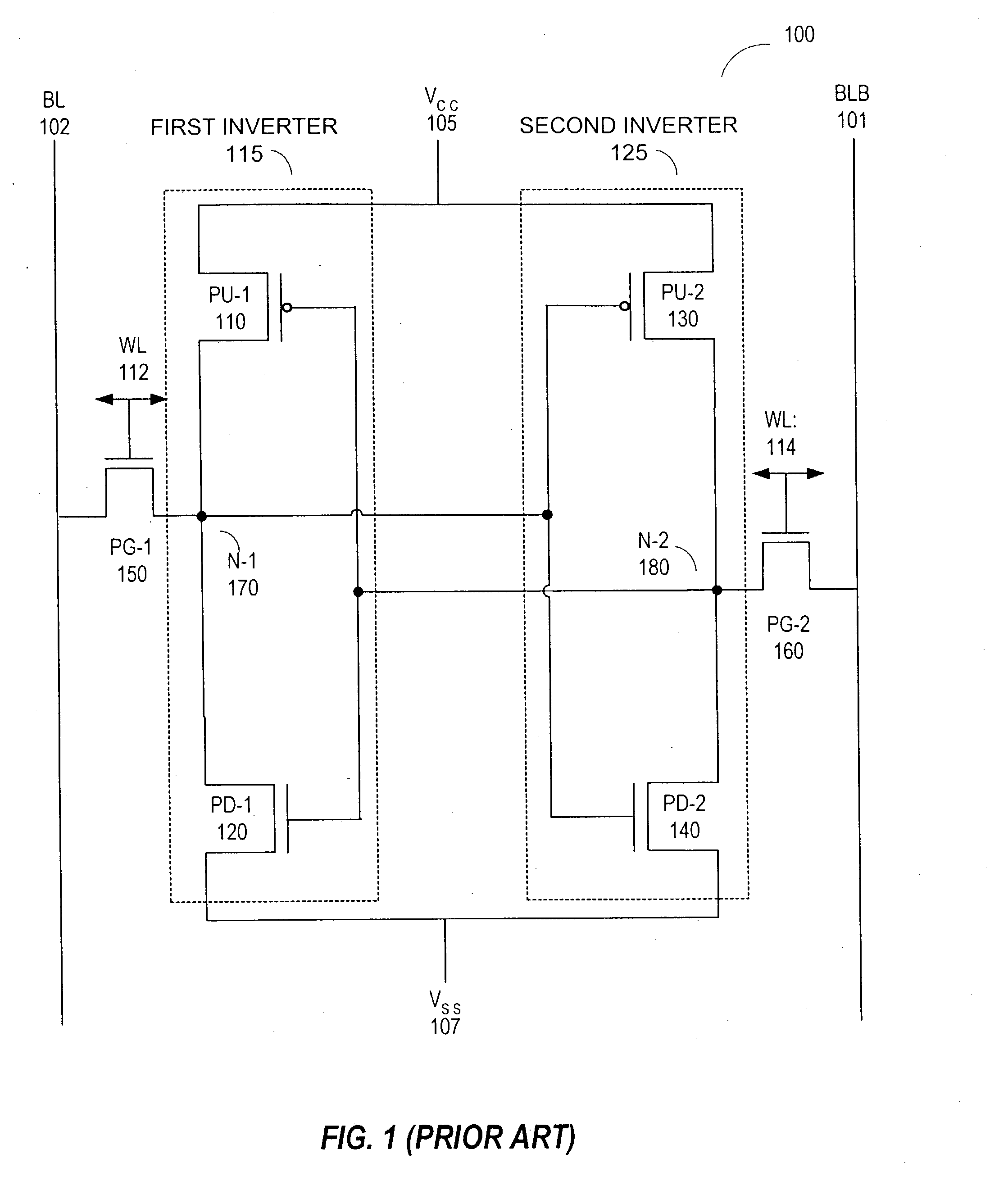
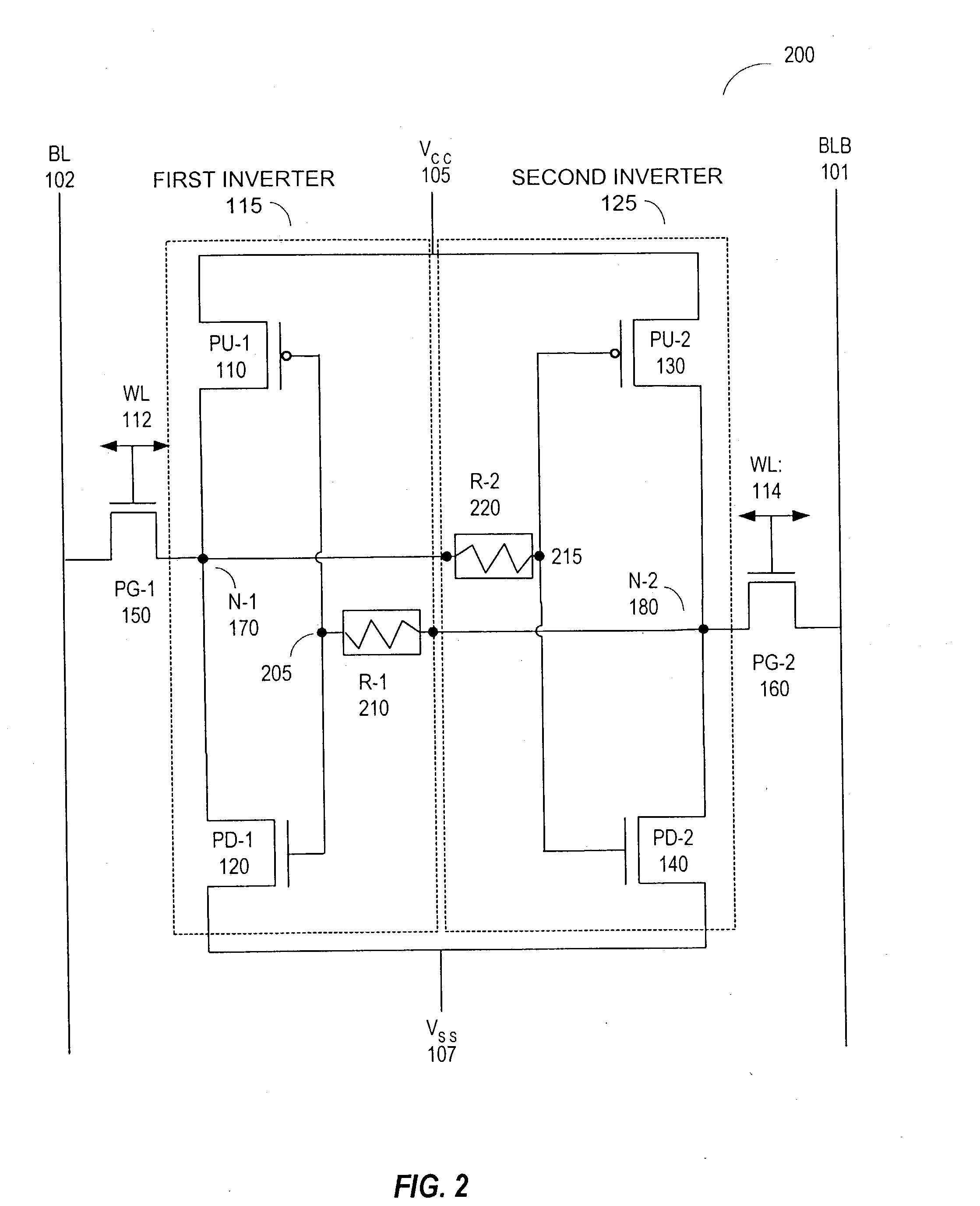
[0022] Elements, which appear in more than one figure herein, are numbered alike in the various figures. The present invention describes an apparatus and method to reduce soft error rate of a SRAM memory cell. According to one form of the invention, a non-silicide poly-1 region is prepared on CMOS gate portion of the SRAM to create a high resistor. The high resistor advantageously causes a delay in depleting charges stored on the memory node...


PUM


Abstract

A high resistor SRAM memory cell to reduce soft error rate includes a first inverter having an output as a first memory node, and a second inverter having an output as a second memory node. The second memory node is coupled to an input of the first inverter through a first resistor. The first memory node is coupled to an input of the second inverter through a second resistor. A pair of access transistors are respectively coupled to a pair of bit lines, a split word line and one of the memory nodes. The resistors are prepared by coating a layer of silicide material on a selective portion of the gate structure of the transistors included in the first inverter, and connecting a portion of the gate structure that is substantially void of the silicide material to the drain of the transistors included in the second inverter.

Description

[0001] 1. Field of the Invention[0002] The present invention relates generally to integrated circuits and methods for memory cells and more particularly to memory cells that offer improved protection against soft errors.[0003] 2. Description of the Relevant Art[0004] Reduced geometry integrated circuit ("IC") chip designs are being adopted to increase the density of devices within integrated circuits, thereby increasing performance and decreasing the cost of the ICs. Modern IC memory chips, such as dynamic random access memory ("DRAM"), static random access memory ("SRAM"), and read only memory ("ROM"), are examples of chips having increasingly higher densities and lower costs. Increases in chip density are primarily accomplished by forming smaller structures within devices and by reducing the separation between devices or between the structures that make up the devices. Typically higher density memory chips often operate under lower voltage levels.[0005] Reduced, sub-micron level g...

Claims


Application Information

Patent Timeline
IPC IPC(8): G11C11/412
CPCG11C11/412
Inventor LIAW, JHON-JHY
Owner TAIWAN SEMICON MFG CO LTD
Why Eureka
Try Eureka