Nonvolatile memory device using semiconductor nanocrystals and method of forming same

a technology of semiconductor nanocrystals and memory devices, which is applied in the field of memory devices, can solve the problems of reducing retention times and reliability, affecting the performance of memory devices,

Inactive Publication Date: 2004-12-23
GLOBALFOUNDRIES US INC
View PDF9 Cites 192 Cited by
  • Summary
  • Abstract
  • Description
  • Claims
  • Application Information

AI Technical Summary

Benefits of technology

[0053] With the unique and unobvious combination of exemplary features of the invention, a nanocrystal memory device can be formed in which the nanocrystals can be defined using a self-assembly process.
[0041] Another exemplary feature of the present invention is to form a nanocrystal memory device in which a self-assembled material is used to template or define the nanocrystals, and allowing good control over the uniformity of the size of the nanocrystal particles, and over their distribution (e.g., where the nanocrystals are located and the spacing between them).
[0043] In a second exemplary aspect of the present invention, a field effect transistor, includes a source region and a drain region formed in a semiconductor material, a channel region disposed between the source region and the drain region, an insulating layer of electrically insulating material disposed over the channel region, a floating gate layer of electrically conducting material disposed over the insulating layer, a layer of electrically insulating material disposed over the floating gate layer, and a gate electrode overlying the layer of insulating material. The floating gate layer includes discrete nanoparticles whose dimensions and distribution are defined by a self-assembling material.

Problems solved by technology

The pathway to many of these density and performance benefits involves scaling the memory FET, which is becoming increasingly difficult.
Also, thinning the program oxide 105 thickness in order to achieve lower write / erase voltages (and thus lower power) has the effect of reducing retention times and reliability.
In a flash device, such leakage will deplete charge from the entire floating gate, resulting in a loss of memory (e.g., in the same way as stress-induced leakage currents compromise the device).
However, none has defined all nanocrystals to be of similar size by using a self-assembly technique.
However, in each of these conventional demonstrations, the nanocrystal sizes were not well-defined, thereby leading to limitations on device performance improvements.
Additionally, as mentioned above and prior to the present invention, nanocrystal floating gate memories have been difficult to use for multi-bit memory applications, because of the large nanocrystal size distributions.
Moreover, there has been no technique which produces a nanocrystal memory device having nanocrystal size distributions which are substantially uniform, using a self-assembly technique.
In sum, the conventional techniques (and subsequently the resulting structure) to make a nanocrystal memory have been notoriously unreliable, and it has been difficult to obtain uniform size of the nanocrystals, and difficult to control the spacing of the distribution around the sample, each of which impact the performance of the device.

Method used


Image

  • Nonvolatile memory device using semiconductor nanocrystals and method of forming same
  • Nonvolatile memory device using semiconductor nanocrystals and method of forming same
  • Nonvolatile memory device using semiconductor nanocrystals and method of forming same

Examples


Embodiment Construction

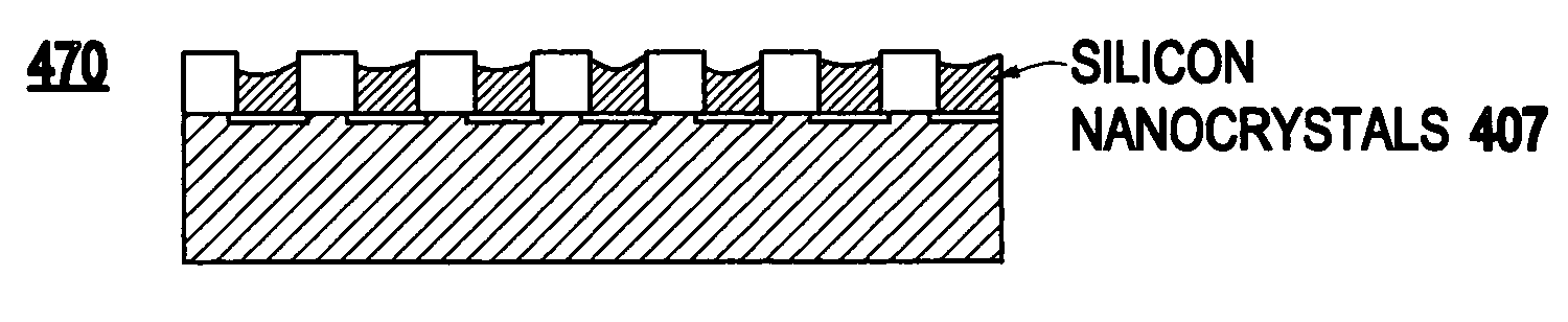
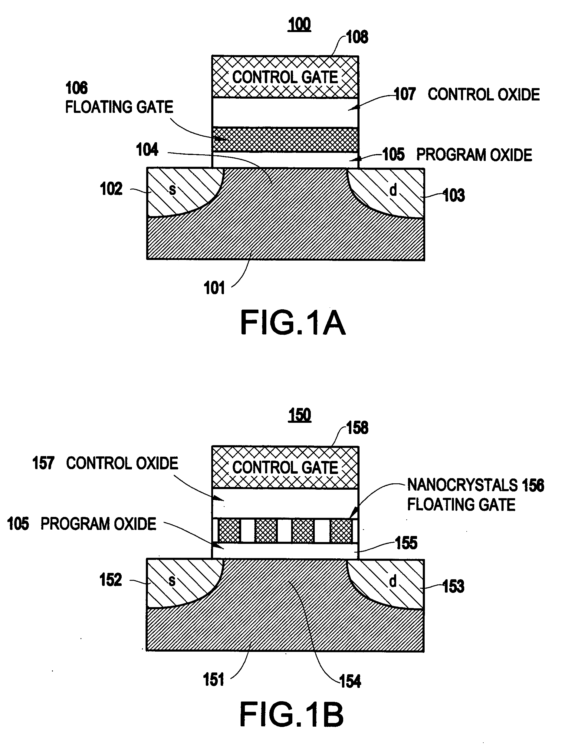
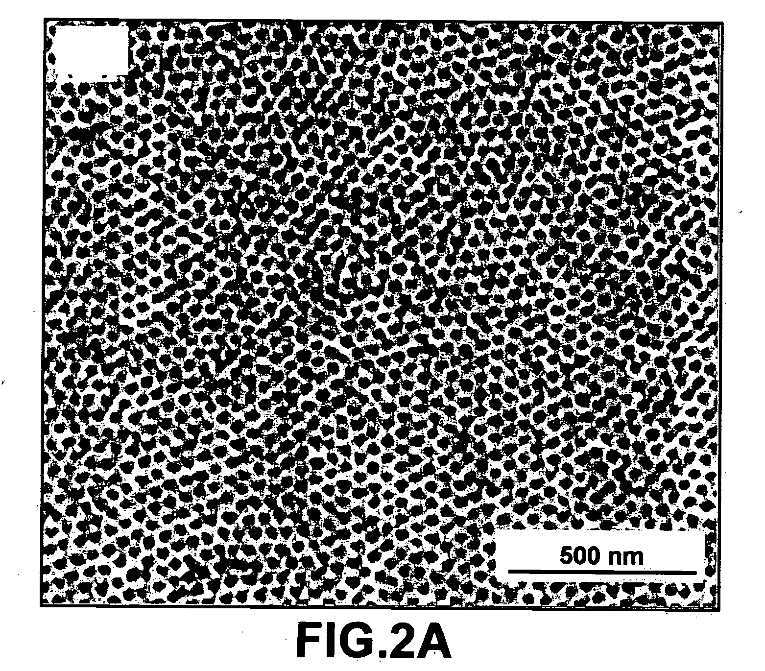
[0081] Referring now to the drawings, and more particularly to FIGS. 2-4(j), there are shown exemplary embodiments of the method and structures according to the present invention.

Exemplary Embodiment

[0082] First, hereinbelow is described an exemplary method for making dense silicon nanocrystal arrays based on self-assembly according to the present invention.

[0083] It is noted that, while a diblock copolymer is described exemplarily below, the invention is not limited to such materials as would be known by one of ordinary skill in the art, taking the present invention as a whole.

[0084] That is, the invention can generally take advantage of self-assembling materials which are not exclusively the particular diblock copolymers described below. There are a variety of different material which naturally form regular arrays, thereby allowing the invention to take advantage of the scale in self-assembling materials. Indeed, there are nanoparticles which self-assemble, there are proteins whic...


PUM

PropertyMeasurementUnit
size distributionsaaaaaaaaaa
thicknessaaaaaaaaaa
diameteraaaaaaaaaa

Abstract

A floating gate for a field effect transistor (and method for forming the same and method of forming a uniform nanoparticle array), includes a plurality of discrete nanoparticles in which at least one of a size, spacing, and density of the nanoparticles is one of templated and defined by a self-assembled material.

Description

[0001] 1. Field of the Invention[0002] The present invention generally relates to a memory device, and more particularly to a nonvolatile memory device using semiconductor crystals and a method for making the same.[0003] 2. Description of the Related Art[0004] Nonvolatile memory is ubiquitous in today's technology-laden world, and the most prevalent type of device used to store information is the flash memory.[0005] In addition to the need for integrated nonvolatile memory in logic systems, there is a large (and rapidly increasing) market for flash memories as stand-alone storage elements. Cellular telephones and digital cameras are several examples of devices which benefit from nonvolatile flash memory cards.[0006] There are various forecasts predicting increased future markets for this type of storage (e.g., see P. Pavan, R. Bez, P. Olivio, and E. Zanoni, IEEE Proc. 85 1248 (1997).[0007] Flash memory is based on the concept of a field effect transistor (FET) whose threshold voltag...

Claims


Application Information

Patent Timeline
Patent Type & Authority Applications(United States)
IPC IPC(8): H01L21/28H01L29/423H01L29/788H01L29/792
CPCB82Y10/00Y10S977/893H01L21/28273H01L21/28282H01L29/42332H01L29/7887H01L29/7923Y10S977/78Y10S438/947Y10S977/883Y10S977/783Y10S977/888Y10S977/856Y10S977/813G11C2216/06H01L29/40114H01L29/40117H01L21/02118H01L21/02227H01L21/02532H01L21/02636H01L21/31111H01L29/66825
Inventor BLACK, CHARLES T.GUARINI, KATHRYN WILDER
Owner GLOBALFOUNDRIES US INC
Why Eureka
Try Eureka