Bypass filter, multi-band antenna switch circuit, and layered module composite part and communication device using them

a technology of antenna switch circuit and composite part, which is applied in the direction of waveguide type devices, electrical equipment, multiple-port networks, etc., can solve the problems of unsuitably large volume and weight of mobile communication devices, unsuitable mobile phone connections, and difficult to secure matching in a wide band from 900 mhz to 1.8 ghz, so as to increase the number of matching parts and facilitate the matching in the entire circuit

Inactive Publication Date: 2004-12-30
MURATA MFG CO LTD
View PDF9 Cites 210 Cited by
  • Summary
  • Abstract
  • Description
  • Claims
  • Application Information

AI Technical Summary

Benefits of technology

0087] Another example of the electrostatic-surge-removing highpass filter circuit of the present invention is shown in FIG. 2. In FIG. 2, the first inductor L1, the second inductor L2, the first capacitor C1 and the second capacitor C2 have the same functions as above. The circuit shown in FIG. 2 is different from that shown in FIG. 1, in that a parallel resonance circuit constituted by a third capacitor C3 and a third inductor L3 is disposed between the first capacitor C1 and an output terminal P2. This parallel resonance circuit can function as a notch filter, which can remove ha

Problems solved by technology

According to recent rapid expansion of mobile phones, however, a frequency band allocated to each system cannot allow all users to use their mobile phones in major cities in advanced countries, resulting in difficulty in connection and thus causing such a problem that mobile phones are sometimes disconnected during communication.
Accordingly, such mobile communications devices are not only expensive but also have unsuitably large volume and weight.
(1) Breakdown of High-Frequency Parts by Electrostatic Surge High-frequency parts such as pin diodes, FET switches, etc. used in the high-frequency switch circuits shown in FIGS. 30 and 31 are vulnerable to electrostatic charge. Particularly in the case of mobile phones, the above high-frequency parts are subjected to breakdown when electrostatic surge from human bodies is input into antennas. In addition, though an antenna switch module per se is not subjected to breakdown, circuits connected downstream of the antenna switch module, such as power amplifiers and low-noise amplifiers, etc. connected to transmission terminals and receiving terminals, respectively, of the antenna switch module are likely subjected to breakdown. Therefore, measures for electrostatic surge have been important.
When an inductor of 5 nH or less is connected to an antenna top, however, it is difficult to secure matching in a wide band from 900 MHz to 1.8 GHz.
Attenuation near 300 MHz is actually as small as 5 dB or less in this circuit, insufficient for the removal of electrostatic surge.
However, the insertion of an LC filter comprising an inductor L1 and a capacitor C1 in each of the antenna terminal, the transmission terminal and the receiving terminal not only prevents the miniaturization and cost reduction of a high-frequency switch, but also causes the deterioration of insertion loss.
Attenuation near 300 MHz is actually as small as about 5 dB in this circuit, insufficient for the removal of electrostatic surge.
Though it may be considered to use varistor diodes and Zener diodes as electrostatic-surge-removing parts, it necessitates a large

Method used


Image

  • Bypass filter, multi-band antenna switch circuit, and layered module composite part and communication device using them
  • Bypass filter, multi-band antenna switch circuit, and layered module composite part and communication device using them
  • Bypass filter, multi-band antenna switch circuit, and layered module composite part and communication device using them

Examples


example 2

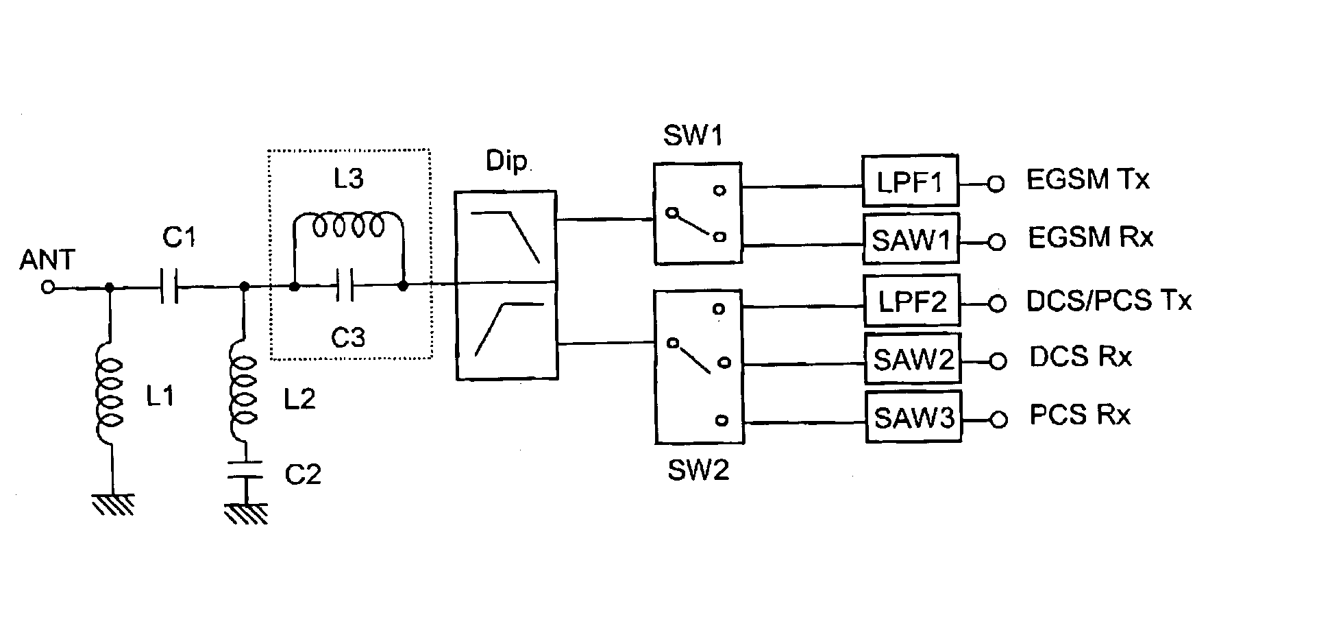
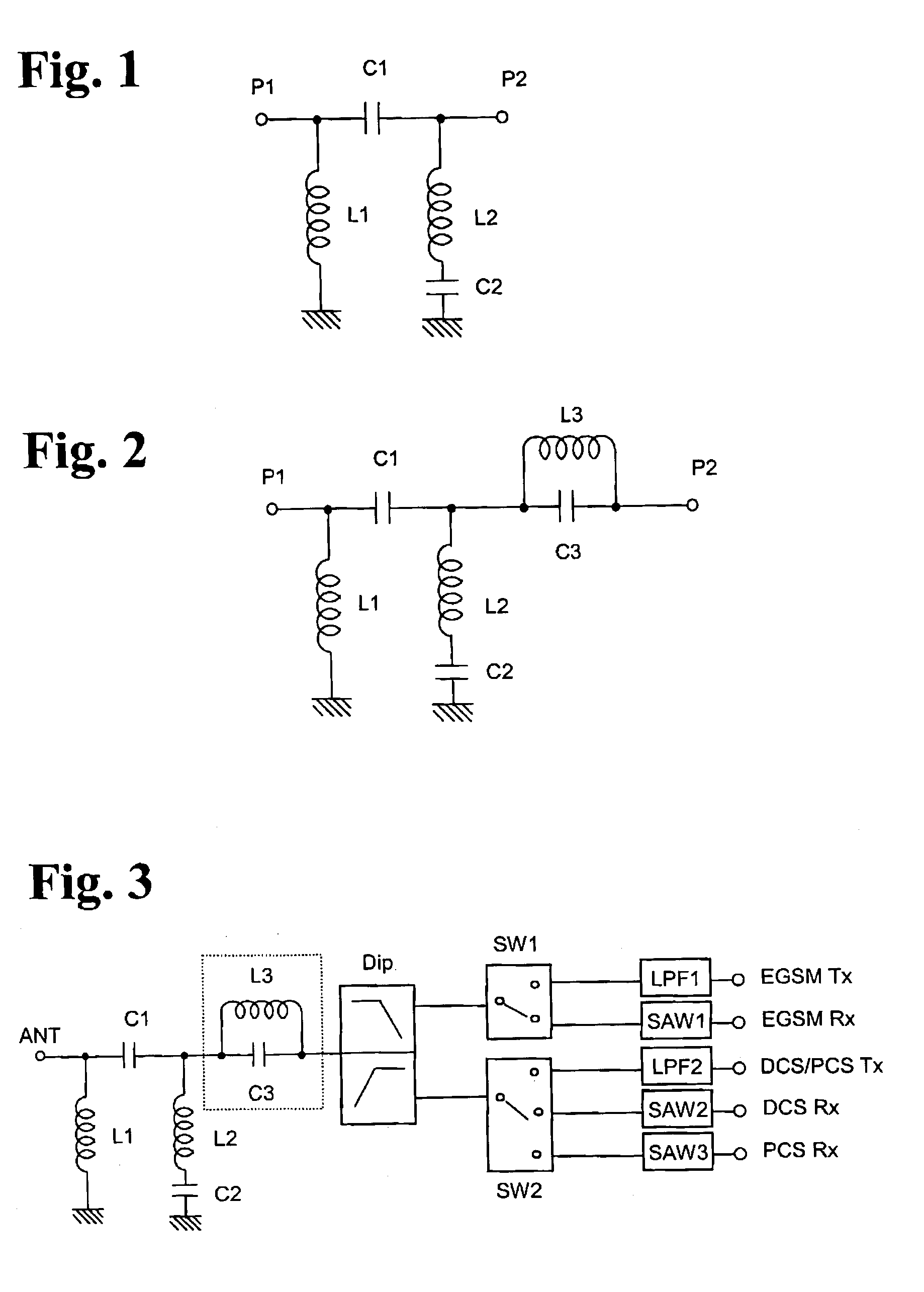
[0098] FIG. 9 is a block diagram showing a tripleband antenna switch circuit adapted for EGSM, DCS and W-CDMA according to one embodiment of the present invention. Branched by the diplexer Dip are signals from the antenna in a band of 880 to 960 MHz for EGSM (transmission frequency: 880 to 915 MHz, receiving frequency: 925 to 960 MHz), and in a band of 1710 to 2170 MHz for DCS (transmission frequency: 1710 to 1785 MHz, receiving frequency: 1805 to 1880 MHz) and W-CDMA (transmission frequency: 1920 to 1980 MHz, receiving frequency: 2110 to 2170 MHz).

[0099] The switch circuit SW1 switches EGSM signals branched by the diplexer Dip to the transmission terminal EGSM Tx and the receiving terminal EGSM Rx. The switch circuit SW2 switches DCS or W-CDMA signals branched by the diplexer Dip to the transmission terminal DCS Tx, the receiving terminal DCS Rx and the transmitting / receiving terminal W-CDMA. To suppress n-th harmonic strain included in transmission signals sent from the power ampl...

example 3

[0117] FIG. 11 is a block diagram showing an antenna switch circuit adapted for EGSM, DCS and W-CDMA. The circuit of this Example is the circuit shown in FIG. 9, in which a first notch filter NF1 is disposed between the diplexer Dip and the first switch circuit SW1. The notch filter NF1 may comprise a parallel resonance circuit and / or a serial resonance circuit shown in FIGS. 14(a) and 14(b), respectively. In this case, the resonance frequency is preferably set to be two or three times the transmission frequency of EGSM. Because the notch filter NF1 removes harmonic strain generated at the first high-frequency switch SW1 in this Example, harmonics generated by the antenna is further suppressed.

example 4

[0118] FIG. 12 is a block diagram showing an antenna switch circuit adapted for EGSM, DCS and W-CDMA with a notch filter NF disposed between the antenna terminal ANT and the diplexer Dip. Other than a switch circuit using a pin diode, a GaAs switch called SPDT (single pole dual throw) is usable as the first switch circuit SW1, and a GaAs switch called SP3T (single pole 3 throw) is usable as the second switch circuit SW2. The notch filter NF1 may be a parallel resonance circuit or a serial resonance circuit shown in FIGS. 14(a) and 14(b), respectively. In this case, the resonance frequency is preferably set to be two or three times the transmission frequency of W-CDMA.

[0119] Because the notch filter NF removes harmonic strain generated by the second high-frequency switch SW2 in this Example, the generation of harmonics by the antenna is suppressed. When the resonance frequency of the notch filter NF is 3.9 GHz, two times the W-CDMA transmission frequency, the attenuation peak can be ...


PUM


Abstract

A multi-band antenna switch circuit including a diplexer connected to an antenna terminal for demultiplexing signals of different passing bands, a first and a second switch circuit for switching a high frequency signal and a low frequency signal demultiplexed by the diplexer to a plurality of transmission/reception terminals, a first and a second low pass filter connected to a transmission path between the diplexer and the transmission terminal or between the first and the second switch circuit and the transmission terminal, and a notch filter provided between the diplexer and the first switch circuit or between the diplexer and the second switch circuit. The multi-band antenna switch circuit includes a high pass filter having an input terminal and an output terminal and provided at least between die diplexer and the antenna terminal and including a first inductor connected between the input terminal and the ground, a first capacitor connected between the input terminal and the output terminal, a second inductor connected to the output terminal, and a second capacitor connected between the second inductor and the ground.

Description

[0001] The present invention relates to a wireless communications system connected to a common antenna for transmitting and receiving two or more signals having different frequencies, particularly to a multiband antenna switch circuit, and a composite laminate multiband antenna switch module and a communications device both comprising the multiband antenna switch circuit.[0002] There are various systems for mobile phones, for instance, EGSM (extended global system for mobile communications) and DCS (digital cellular system) widely used mostly in Europe, PCS (personal communications services) used in the U.S., and various systems using TDMA (time division multiple access) such as PDC (personal digital cellular) used in Japan. According to recent rapid expansion of mobile phones, however, a frequency band allocated to each system cannot allow all users to use their mobile phones in major cities in advanced countries, resulting in difficulty in connection and thus causing such a proble...

Claims


Application Information

Patent Timeline
IPC IPC(8): H03H7/01H03H7/075H03H7/46H04B1/40H04B1/44H04B1/48H04B1/52
CPCH03H7/0115H03H7/0153H03H7/1758H03H7/1766H03H7/1783H03H7/465H03H2001/0085H04B1/0057H04B1/006H04B1/406H04B1/44H04B1/48H04B1/52
Inventor FUKAMACHI, KEISUKEKEMMOCHI, SHIGERUWATANABE, MITSUHIROTAKETA, TSUYOSHITAI, HIROYUKIYOKOUCHI, SATORU
Owner MURATA MFG CO LTD
Why Eureka
Try Eureka