Upper electrode and plasma processing apparatus

a plasma processing and upper electrode technology, applied in plasma technology, energy-based chemical/physical/physical-chemical processes, pressurized chemical processes, etc., can solve the problems of increasing thermal conductivity deterioration, and high cost of the entire upper electrode, so as to reduce an overall running cost, improve temperature controllability, and high accuracy

Inactive Publication Date: 2005-01-06
TOKYO ELECTRON LTD
View PDF10 Cites 47 Cited by
  • Summary
  • Abstract
  • Description
  • Claims
  • Application Information

AI Technical Summary

Benefits of technology

[0011] It is, therefore, an object of the present invention to provide a plasma processing apparatus and an upper electrode employed therein, which are capable of performing a plasma process with high accu

Problems solved by technology

However, a replacement of the entire upper electrode, including even the non-defective parts incurs high cost, resulting in an increase in an overall running cost.
However, in such case of the

Method used


Image

  • Upper electrode and plasma processing apparatus
  • Upper electrode and plasma processing apparatus
  • Upper electrode and plasma processing apparatus

Examples


Embodiment Construction

[0020] Hereinafter, preferred embodiments of the present invention will be described with reference to the accompanying drawings.

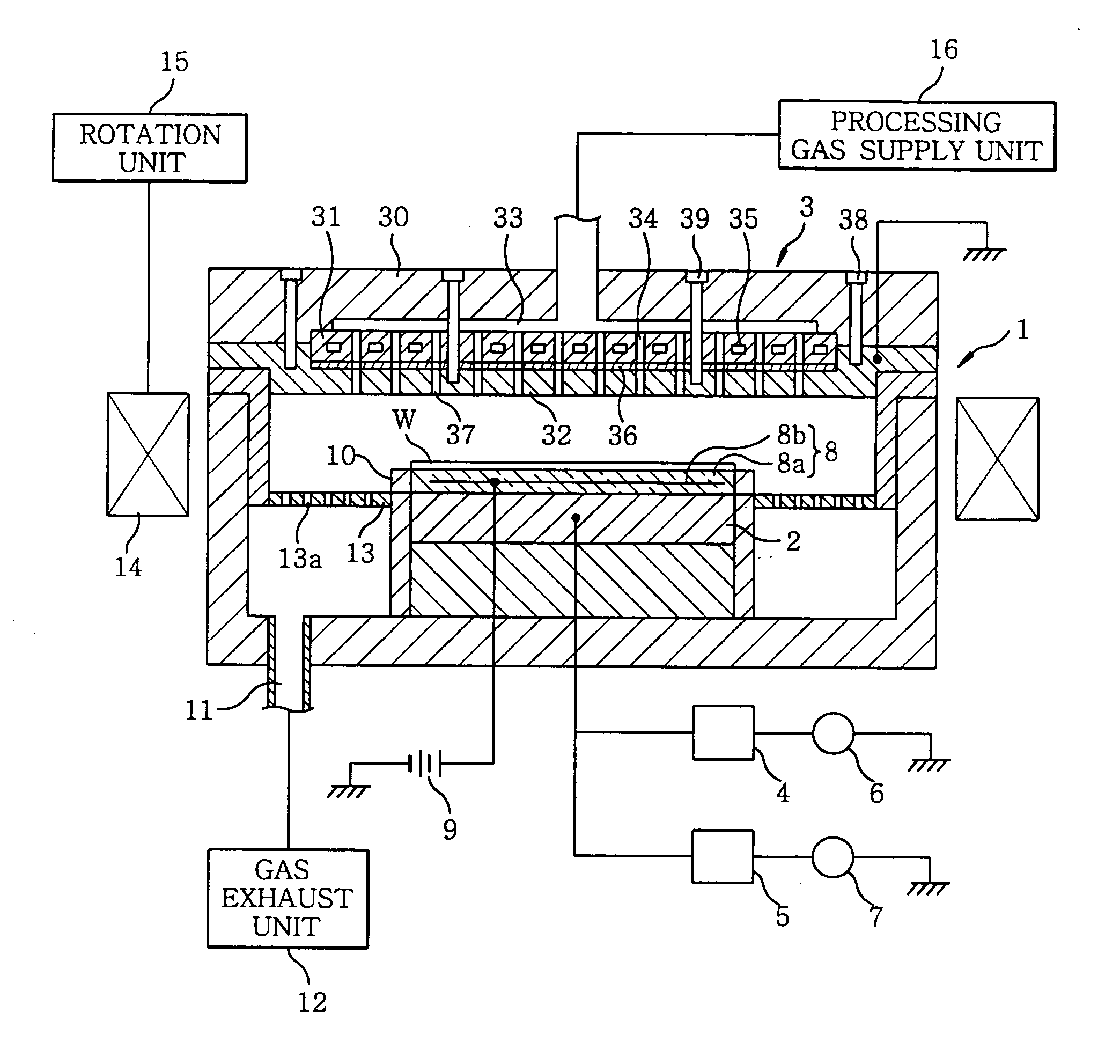
[0021] Referring to FIG. 1, there is schematically illustrated a configuration of a preferred embodiment in which the present invention is applied to a plasma etching apparatus for etching a semiconductor wafer. As shown in FIG. 1, a reference numeral 1 represents a cylindrical vacuum chamber, made of, e.g., aluminum, which can be hermetically sealed.

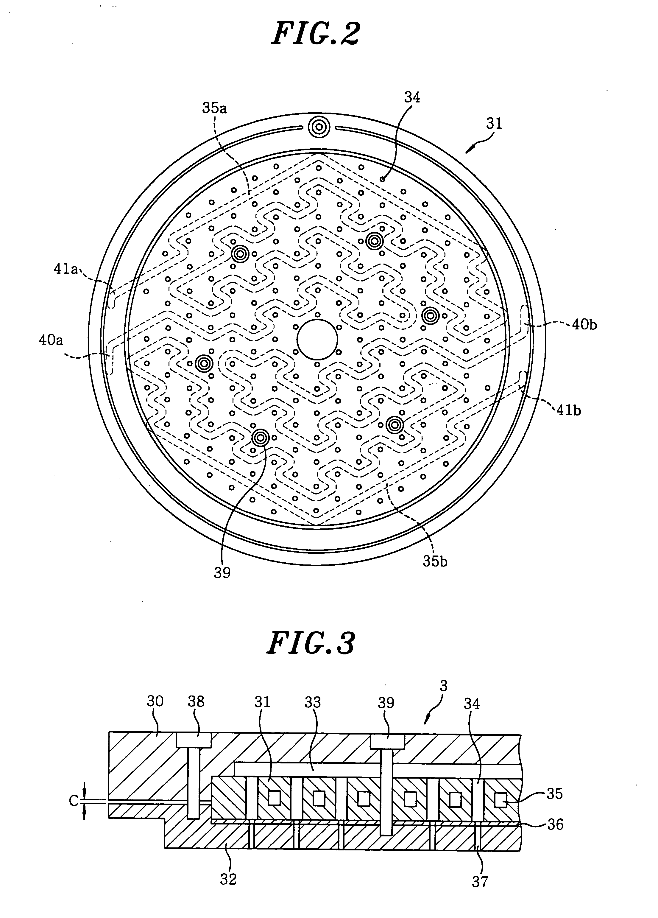
[0022] Installed in the vacuum chamber 1 is a mounting table 2 for mounting thereon a semiconductor wafer W, which also serves as a lower electrode. Furthermore, installed at a ceiling portion of the vacuum chamber 1 is an upper electrode 3, which makes up a shower head. The mounting table 2 (the lower electrode) and the upper electrode 3 form a pair of parallel plate electrodes. A structure of the upper electrode 3 will be described later.

[0023] The mounting table 2 is connected with two high frequency pow...


PUM

PropertyMeasurementUnit
Lengthaaaaaaaaaa
Flow rateaaaaaaaaaa
Flexibilityaaaaaaaaaa

Abstract

An upper electrode for use in generating a plasma of a processing gas includes a cooling block having a coolant path for circulating a coolant therethrough and one or more through holes for passing the processing gas therethrough, an electrode plate having one or more injection openings for injecting the processing gas toward the substrate to be processed mounted on the mounting table, and an electrode frame installed at an upper portion of the cooling block and providing a processing gas diffusion gap for diffusing the processing gas between the cooling block and the electrode frame. The electrode plate is detachably fixed to a bottom surface of the cooling block via a thermally conductive member having flexibility.

Description

FIELD OF THE INVENTION [0001] The present invention relates to a plasma processing apparatus for performing a plasma process such as an etching process, a film forming process and the like by inducing a plasma to act on a substrate to be processed, e.g., a semiconductor wafer, a glass substrate for liquid crystal display (LCD) or the like; and an upper electrode employed therein. BACKGROUND OF THE INVENTION [0002] Conventionally, a plasma processing apparatus for performing a process such as an etching process, a film forming process and the like by generating a plasma in a vacuum chamber and inducing the plasma to act on a substrate to be processed, e.g., a semiconductor wafer, a glass substrate for LCD or the like, has been widely used in a field of manufacturing semiconductor devices. [0003] In such a plasma processing apparatus, e.g., a so-called parallel plate type plasma processing apparatus, a mounting table (a lower electrode) for mounting thereon a semiconductor wafer and t...

Claims


Application Information

Patent Timeline
IPC IPC(8): B01J3/00H05H1/46B01J19/08C23C16/44C23C16/455C23C16/509C23F4/00H01J37/32H01L21/02H01L21/3065
CPCC23C16/45565C23C16/5096H01J37/32724H01J37/3244H01J37/32009H01L21/02
Inventor HAYASHI, DAISUKEISHIDA, TOSHIFUMIKIMURA, SHIGETOSHI
Owner TOKYO ELECTRON LTD
Why Eureka
Try Eureka