Self-assembly methods for the fabrication of McFarland-Tang photovoltaic devices

a technology of photovoltaic devices and self-assembly methods, which is applied in the direction of material nanotechnology, electrolytic capacitors, nanotechnology, etc., can solve the problems of high cost of building and operation, limited material types, and high cost of film materials manufactured in large manufacturing facilities

Inactive Publication Date: 2005-01-06
NANOSCALE MATERIALS
View PDF3 Cites 41 Cited by
  • Summary
  • Abstract
  • Description
  • Claims
  • Application Information

AI Technical Summary

Problems solved by technology

These self-assembly processes, however, while highly advantageous, generally are limited with respect to the types of materials that can be deposited by a particular process, by costs and manufacturing facilities.
Presently, film materials are manufactured in large manufacturing facilities that are expensive to buil

Method used


Image

  • Self-assembly methods for the fabrication of McFarland-Tang photovoltaic devices
  • Self-assembly methods for the fabrication of McFarland-Tang photovoltaic devices
  • Self-assembly methods for the fabrication of McFarland-Tang photovoltaic devices

Examples


example 1

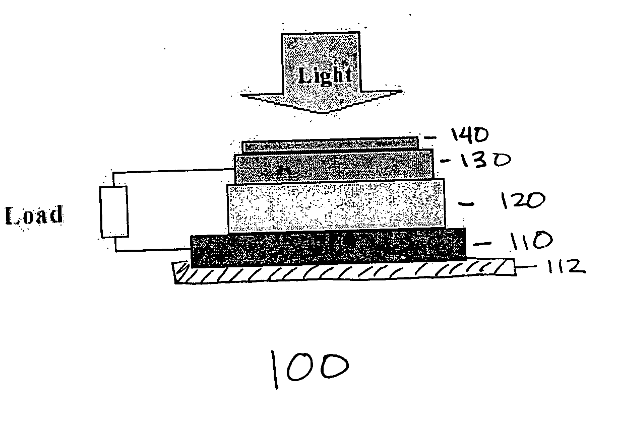
InP Q-Dot Sensitized Au / TiO2 / Ti on a Silicon Substrate McFarland-Tang Solar Cell

[0054] In this example a McFarland-Tang solar cell built on a silicon substrate is described. In this device, a Ti layer was deposited on a silicon substrate using a vacuum deposition method in a thickness of about 50 nm. A TiO2 anatase thin film was self-assembled using the layer-by-layer ESA methodology of the present invention using a 15 nm TiO2 anatase as the nanoparticle and 3-MPS (3-mercapto-1-propanesulfonic acid sodium salt) as the polyelectrolyte. A 30 nm Au film was then self-assembled on the TiO2 layer by the NISA method of the present invention using HAuCl4 as the gold source and NaHB4 as the reduction agent. A monolayer of bi-functional thiol molecules was used to modify the surface of the Au film to enhance the up taking of the InP Q-dots. A solar simulator was used as the light source to illuminate the device from the InP Q-dot film side.

[0055] Tuning the Q-dot particle size resulted in ...

example 2

Change in Thickness of Components Results in Different PV Response

[0057] A self-assembled McFarland-Tang solar cell built on a silicon substrate is described in this example. In this device, a Ti layer was deposited on a silicon substrate using a vacuum deposition method to a thickness of about 150 m and used as the electrode. A TiO2 anatase thin film of about 200 m was self-assembled using the layer-by-layer ESA methodology of the present invention using a 15 m TiO2 anatase as the nanoparticle and 3-MPS as the polyelectrolyte. A 100 nm Au film was then self-assembled on the TiO2 layer by the NISA method of the present invention using HAuCl4 as the gold source and NaHB4 as the reduction agent. A monolayer of bi-functional thiol molecules was used to modify the surface of the Au film to enhance the up taking of the InP Q-dots which had a thickness of about 80 nm.

[0058] A solar simulator was used as the light source to illuminate the device from the InP Q-dot film side. FIG. 7 illus...


PUM


Abstract

The present invention relates to self-assembly methodologies, such as electrostatic self-assembly, layer by layer covalent self-assembly, nuclear induced self-assembly, regular ink jet printing and self-assembly inkjet printing methodologies for the fabrication of McFarland-Tang multilayer structured photovoltaic devices, photo-detectors and sensors. The methodology of the present invention allows for the flexibility to nanofabricate the thin layer of the semiconductor layer, the ultra-thin noble metal layer, and the ultra-thin photosensitizer layers to form the desired multilayer photovoltaic devices. Extending the self-assembly processes by ink-jet printing allows for the up-scaled nano-manufacture of McFarland-Tang photovoltaic devices on any type of substrate, including light-weight flexible photovoltaic fabrics and paper.

Description

CROSS-REFERENCE TO RELATED APPLICATIONS [0001] The present invention is related to and claims the benefit of provisional patent application Ser. No. 60 / 472,580, filed May 22, 2003, which is expressly incorporated fully herein by reference in its entirety.STATEMENT REGARDING FEDERALLY SPONSORED RESEARCH [0002] This invention was made in connection with Government support under Contract number NS2-3175 awarded by the National Science Foundation. The Government has certain rights in the invention.FIELD OF THE INVENTION [0003] This invention concerns the fabrication of McFarland-Tang photovoltaic (PV) devices using self-assembly process, such as dipping methods, self-assembly inkjet printing and regular ink jet printing methods. BACKGROUND OF THE INVENTION [0004] Recent advances in technology have increased the demand for improved material processing with strict tolerances on processing parameters. For example, current integrated circuit technology already requires tolerances on process...

Claims


Application Information

Patent Timeline
IPC IPC(8): H01L21/302H01L31/00
CPCB82Y10/00B82Y30/00H01G9/2031H01G9/2045Y02E10/542H01L31/0392H01L31/07H01L31/18H01G9/205H01L31/03925H01L31/03926
Inventor ZENG, TINGYING
Owner NANOSCALE MATERIALS
Why Eureka
Try Eureka