Semiconductor integrated circuit and method of designing the same

a technology of integrated circuits and semiconductors, applied in the direction of semiconductor devices, semiconductor/solid-state device details, electrical apparatus, etc., can solve the problems of micropatterning difficult to perform, the demand for shortening the development time, and the abrupt increase in the circuit scale of semiconductor integrated circuits

Inactive Publication Date: 2005-01-06
KK TOSHIBA
View PDF2 Cites 78 Cited by
  • Summary
  • Abstract
  • Description
  • Claims
  • Application Information

AI Technical Summary

Problems solved by technology

Recently, the circuit scale of semiconductor integrated circuits is abruptly increasing, and demands for shortening the development time are also increasing.
As micropatterning progresses, however, it is found that the design rule for impurity ion implantation makes micropatterning difficult to perform, compared to the design rule for MOS transistor formation and metal interconnection.
Unfortunately, pin grids are not suited to the cell layout, so intervals between a gate electrode GE11 of a P-channel MOS transistor PM11 and N-channel MOS transistor NM11, a gate electrode GE12 of a P-channel MOS transistor PM12 and N-channel MOS transistor NM12, and a gate electrode GE13 of a P-channel MOS transistor PM13 and N-channel MOS transistor NM13 do not match the pin grids.
This layout difference between the gate electrodes o

Method used


Image

  • Semiconductor integrated circuit and method of designing the same
  • Semiconductor integrated circuit and method of designing the same
  • Semiconductor integrated circuit and method of designing the same

Examples


first embodiment

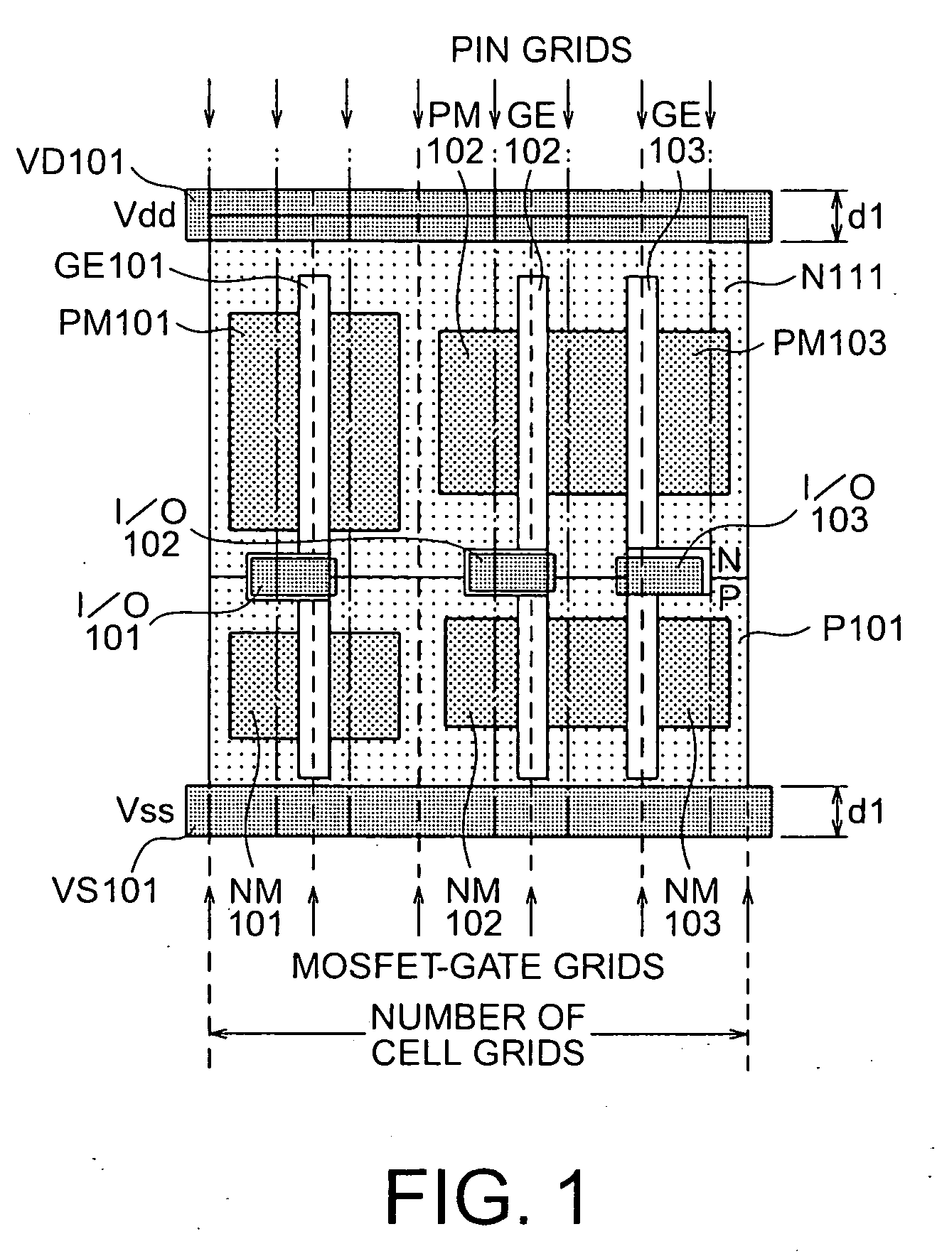
[0048] (1) First Embodiment

[0049]FIG. 1 is a plan view showing the arrangement of a semiconductor integrated circuit according to this embodiment.

[0050] An N-type well region N101 and P-type well region P101 are placed in a surface portion of a semiconductor substrate. A power supply voltage Vdd line VD101 and ground voltage Vss line VS101 are placed above and below, respectively, in FIG. 1, the pair of the N-type well region N101 and P-type well region P101.

[0051] In the vertical direction of FIG. 1, pin grids as a reference of a metal pin pitch are indicated by the alternate long and short dashed lines, and gate grids as a reference of the pitch of the gate electrodes of MOS transistors are indicated by the dotted lines. In this embodiment, the ratio of the pin grid pitch to the gate grid pitch is set at 2:3.

[0052] In the N-type well region N101, a gate electrode GE101 is formed on the substrate, and a P-type impurity is ion-implanted on the two sides of this gate electrode to ...

second embodiment

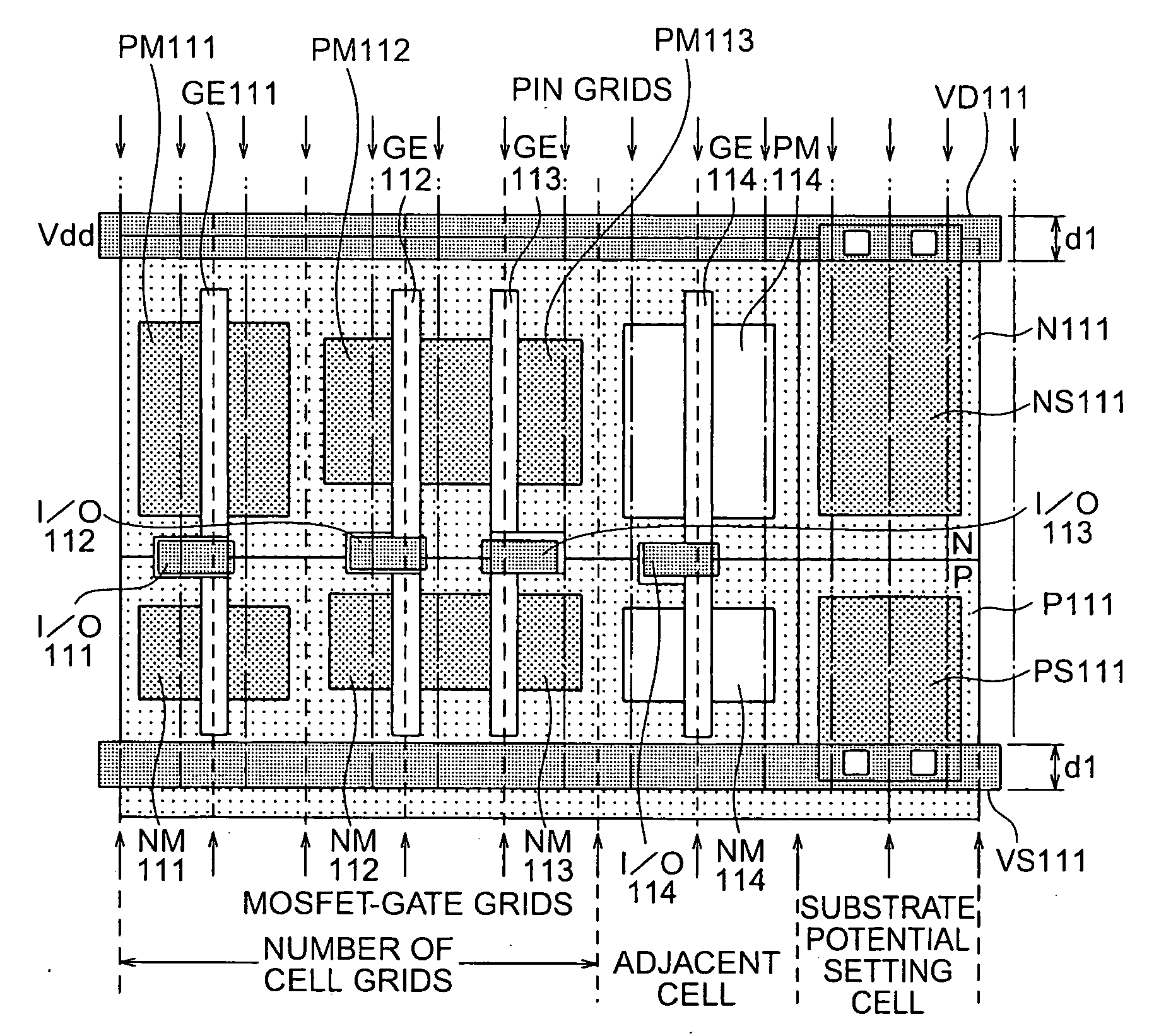
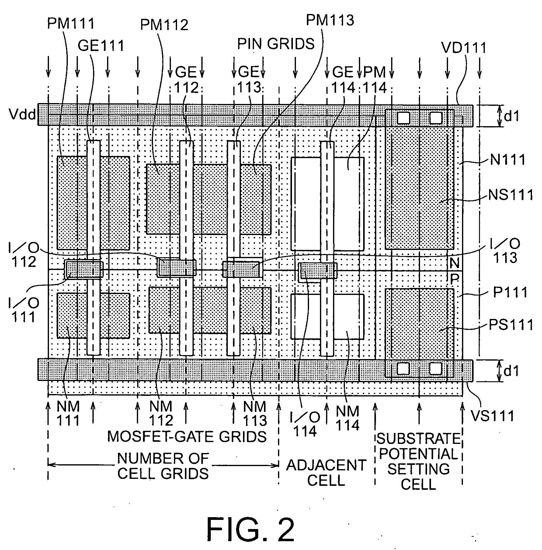
[0062] (2) Second Embodiment

[0063]FIG. 2 is a plan view showing the arrangement of a semiconductor integrated circuit according to this embodiment.

[0064] This embodiment is characterized in that two adjacent cells are placed, and impurity diffusion layers are additionally placed as cells for setting the substrate potential.

[0065] An N-type well region N111 and P-type well region P111 are placed in a surface portion of a semiconductor substrate. A power supply voltage Vdd line VD111 and ground voltage Vss line VS111 are placed above and below, respectively, in FIG. 2, the pair of the N-type well region N111 and P-type well region P111.

[0066] As in the first embodiment described above, in the vertical direction of FIG. 2, pin grids as a reference of a metal pin pitch are indicated by the alternate long and short dashed lines, and gate grids as a reference of the pitch of the gate electrodes of MOS transistors are indicated by the dotted lines. In this embodiment, as in the above em...

third embodiment

[0077] (3) Third Embodiment

[0078]FIG. 3 is a plan view showing the arrangement of a semiconductor integrated circuit according to this embodiment.

[0079] An N-type well region N121 and P-type well region P121 are placed in a surface portion of a semiconductor substrate. A power supply voltage Vdd line VD121 and ground voltage Vss line VS121 are placed above and below, respectively, in FIG. 3, the pair of the N-type well region N121 and P-type well region P121.

[0080] Another pair of a P-type well region P122 and N-type well region N122 are symmetrically placed with respect to the ground voltage Vss line VS121. A power supply voltage Vdd line VD122 is placed below, in FIG. 3, the N-type well region N122.

[0081] As in the first and second embodiments described above, pin grids as a reference of a metal pin pitch are indicated by the alternate long and short dashed lines, and gate grids as a reference of the pitch of the gate electrodes of MOS transistors are indicated by the dotted li...


PUM


Abstract

According to the present invention, a semiconductor integrated circuit having: a cell region in which a plurality of MOS transistors forming at least one cell are placed; and first and second power lines placed along one direction in a peripheral portion of the cell region, wherein in the cell region, gate grids for defining a first pitch in the one direction and pin grids for defining a second pitch in the one direction are set, gate electrodes of the MOS transistors are placed in accordance with the gate grids, and an interconnection layer is placed in accordance with the pin grids.

Description

CROSS REFERENCE TO RELATED APPLICATION [0001] This application is based upon and claims benefit of priority under 35 USC 119 from the Japanese Patent Application No. 2003-136135, filed on May 14, 2003, the entire contents of which are incorporated herein by reference. BACKGROUND OF THE INVENTION [0002] The present invention relates to a semiconductor integrated circuit and a method of designing the same and, more particularly, to a semiconductor integrated circuit suited to laying out standard cells. [0003] Recently, the circuit scale of semiconductor integrated circuits is abruptly increasing, and demands for shortening the development time are also increasing. [0004] Accordingly, a method has been extensively used which does not cause a circuit designer to plan and design a circuit configuration for realizing logic by himself or herself, but designs a circuit block for implementing a desired function by performing logic synthesis, placement, and routing by using software for perfo...

Claims


Application Information

Patent Timeline
IPC IPC(8): H01L21/822H01L21/82H01L27/02H01L27/04H01L27/10H01L27/118H01L29/76H01L29/94H01L31/119
CPCH01L27/11807H01L27/0207
Inventor KOBAYASHI, TSUGUO
Owner KK TOSHIBA
Why Eureka
Try Eureka