
Etching process for micromachining crystalline materials and devices fabricated thereby

a technology of crystalline materials and micromachining, which is applied in the direction of microstructural devices, microstructural technology, liquid/fluent solid measurements, etc., can solve the problems of unacceptable reduction of the benefits of crystallographic planes, unsatisfactory dicing saw cuts, and difficult otherwise achieved assembly economics

Active Publication Date: 2005-01-06
SAMSUNG ELECTRONICS CO LTD
View PDF10 Cites 11 Cited by
  • Summary
  • Abstract
  • Description
  • Claims
  • Application Information

AI Technical Summary

Benefits of technology

[0122] These and other advantages of the present invention will be apparent to those skilled in the art from the foregoing specification. Accordingly, it will be recognized by those skilled in the art that changes or modifications may be made to the above-described embodiments without departing from the broad inventive concepts of the invention. For example, a non-anisotropically etched feature may be formed adjacent an etch-stop pit. It should therefore be understood that this invention is not limited to the particular embodiments described herein, but is intended to include all changes and modifications that are within the scope and spirit of the invention as set forth in the claims.

Problems solved by technology

Thus microsystems can be achieved with assembly economy difficult to otherwise achieve.
While discrete, non-communicating, three-dimensional structures may be conveniently formed by an anisotropic etching, etched structures which communicate with one another at particular geometries, such as a convex corner, pose significant problems for applications in which it is desirable to maintain the precise geometry defined by the crystallographic planes.
Thus, the benefits provided by the crystallographic planes can be unacceptably diminished.
However, dicing saw cuts can be undesirable, because such cuts typically must extend across the entire substrate, or consume an undesirably large portion of it, and may not conveniently be located at discrete locations within the substrate.
Moreover, dicing saw cuts create debris which may be deposited across the substrate surface and lodge within the three-dimensional structures, which may interfere with the precise positioning of optical elements within such a structure.

Method used


Image

  • Etching process for micromachining crystalline materials and devices fabricated thereby
  • Etching process for micromachining crystalline materials and devices fabricated thereby
  • Etching process for micromachining crystalline materials and devices fabricated thereby

Examples


Embodiment Construction

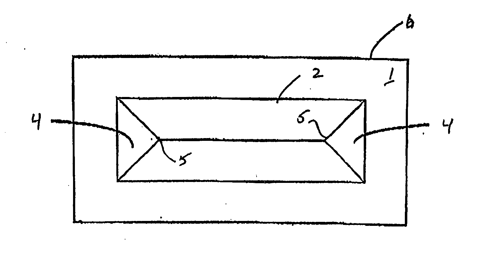
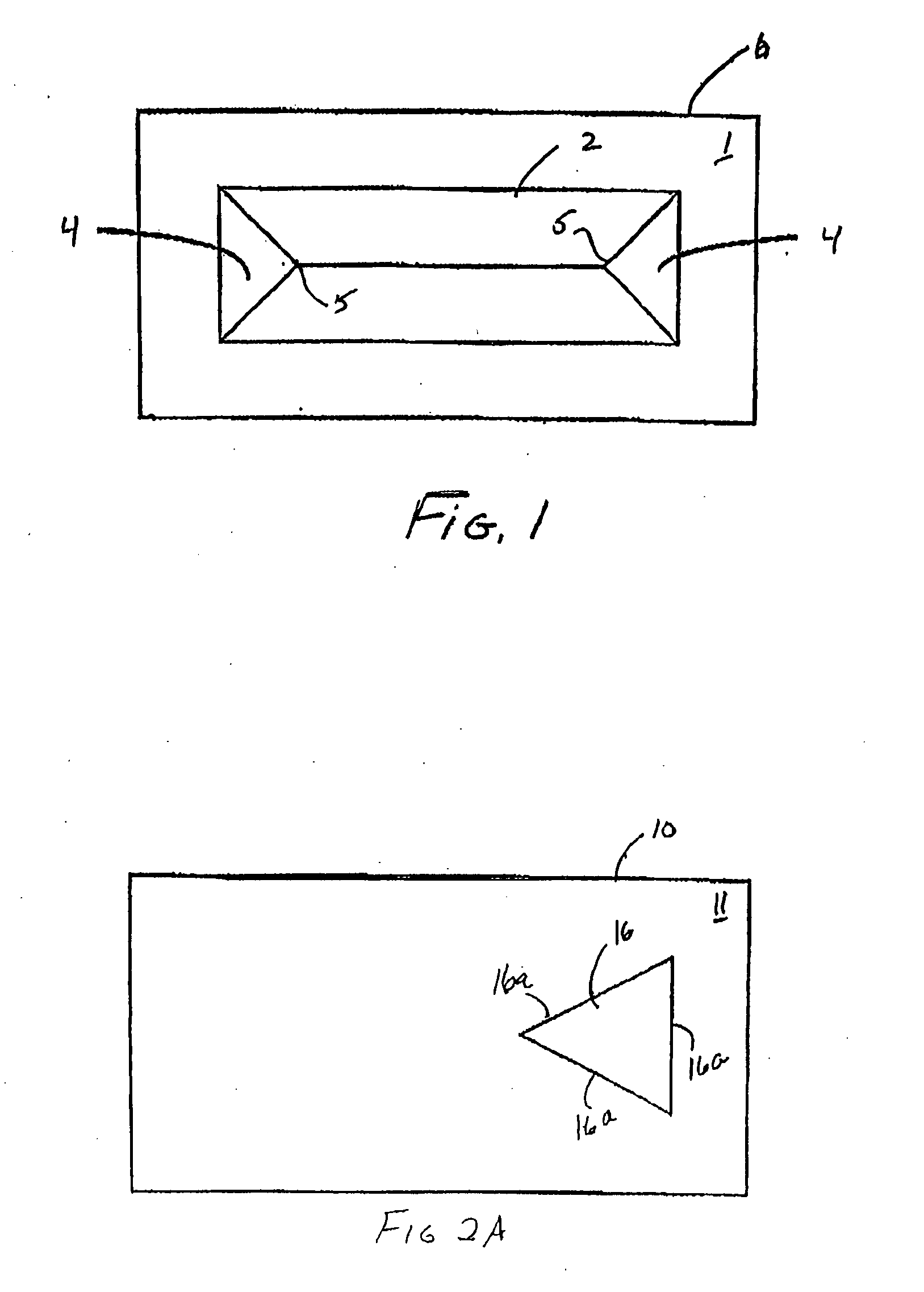
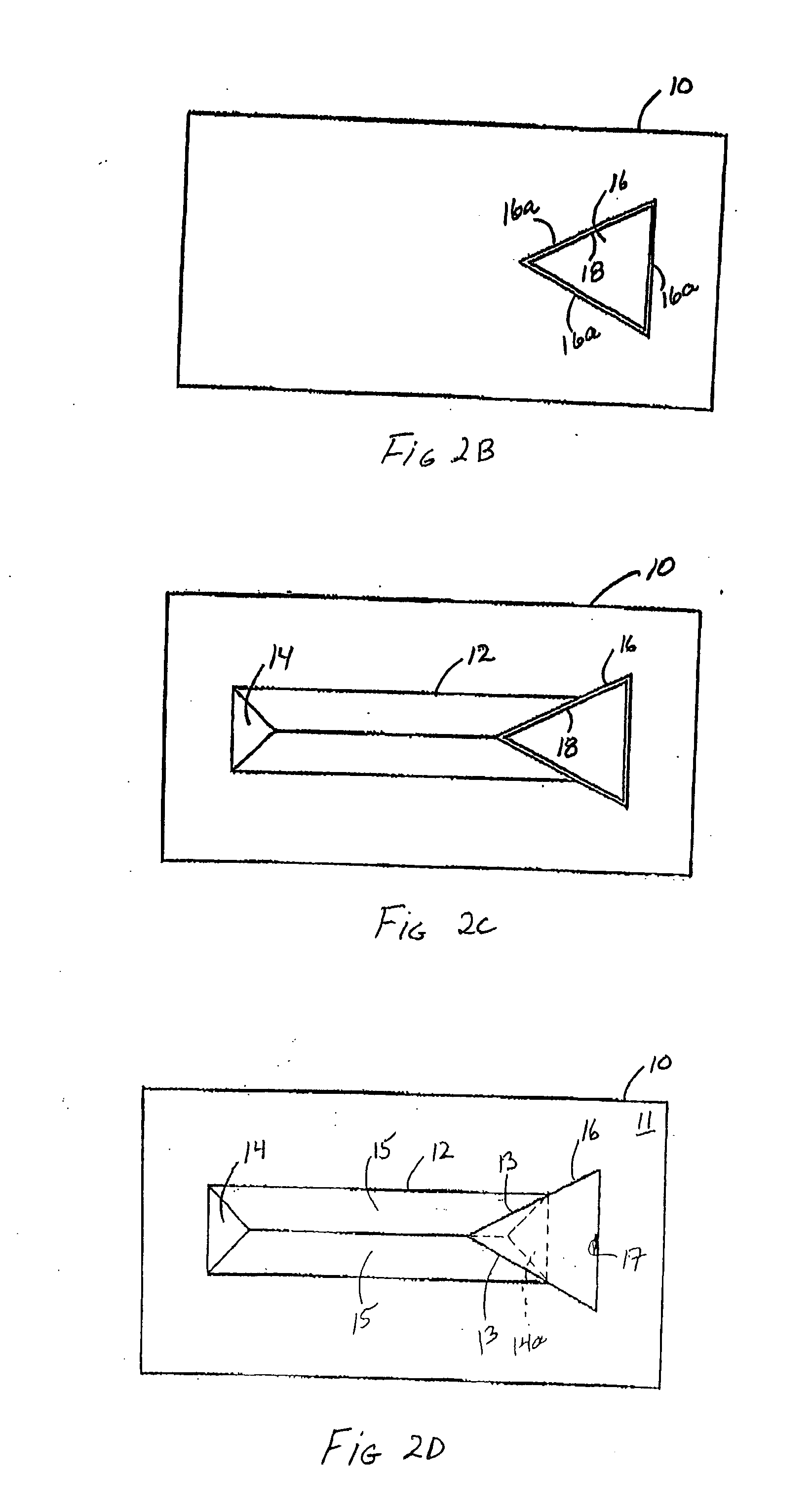
[0055] Referring now to the figures, wherein like elements are numbered alike throughout, several different embodiments of devices in accordance with the present invention are illustrated. The different embodiments include a substrate having at least two common features, an etch-stop pit and an anisotropically etched feature adjacent the etch-stop pit. The etch-stop pit has a shape suited to supporting an etch-stop layer on the surfaces of the etch-stop pit. The etch-stop pit is created prior to creating the anisotropically etched feature. The etch-stop layer comprises a material resistant to the etchant which is used to create the anisotropically etched feature. After the etch-stop layer is provided, the anisotropically etched feature is etched in the substrate. The etch-stop layer prevents the anisotropic etching from extending into the region where the etch-stop pit is located. The prevention of such anisotropic etching by the etch-stop layer provides that the crystallographic pl...


PUM

PropertyMeasurementUnit
Angleaaaaaaaaaa
Areaaaaaaaaaaa

Abstract

The present invention relates generally to micromachining. More particularly, the present invention relates to a method for combining directional ion etching and anisotropic wet etching and devices and structures fabricated thereby. The present invention is particularly applicable to silicon micromachining and provides architectures that combine crystallographic surfaces and vertical dry etched surfaces together in the same structure.

Description

RELATED APPLICATIONS [0001] This application claims the benefit of priority of U.S. Provisional Application No. 60 / 472,910 filed on May 23, 2003 and U.S. Provisional Application No. 60 / 472,909 filed on May 23, 2003, the entire contents of which applications are incorporated herein by reference. This application is related to the subject matter of U.S. application Ser. No. ______, [attorney docket number R&H 04-11] filed on the even date herewith.FIELD OF THE INVENTION [0002] The present invention relates generally to micromachining. More particularly, the present invention relates to a method for combining directional ion etching and anisotropic wet etching and devices and structures fabricated thereby. The present invention is particularly applicable to silicon micromachining. BACKGROUND OF THE INVENTION [0003] The art of bulk micromachining in silicon has changed since the invention of practical means to etch vertical sidewalls in silicon using dry etching technology, as has large...

Claims


Application Information

Patent Timeline
IPC IPC(8): G02B6/42B81B1/00B81C1/00H01L31/00
CPCB81B2201/047G02B6/4214B81C1/00547B81C1/00
Inventor STEINBERG, DAN A.
Owner SAMSUNG ELECTRONICS CO LTD
Learn More