

Adhesion enhanced semiconductor die for mold compound packaging
a technology of mold compound and adhesive bonding die, which is applied in the direction of semiconductor devices, semiconductor/solid-state device details, electrical equipment, etc., can solve the problems of difficult to obtain a good, solid adhesive bond between the die and the package, the oxide on the silicon die substrate does not lend itself to uniform wetting, and the surface of other problems, to achieve the effect of reducing the delamination potential of the die, reducing the cracking of the package, and improving the adhesion of the di
- Summary
- Abstract
- Description
- Claims
- Application Information
AI Technical Summary
Benefits of technology
Problems solved by technology
Method used
Image

Examples
Embodiment Construction
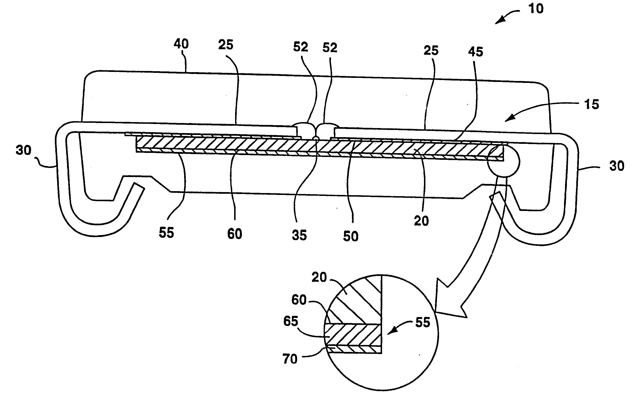
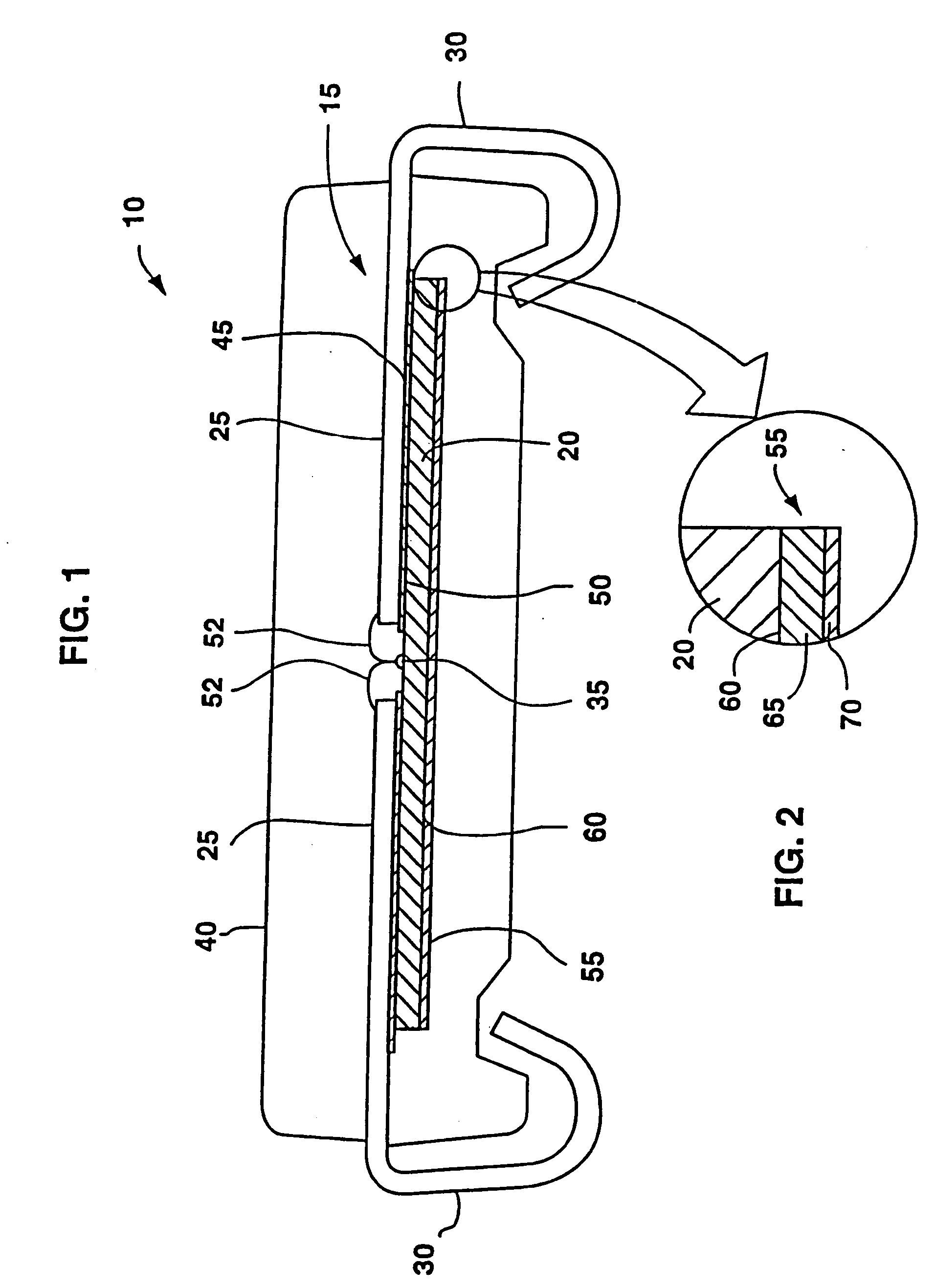
[0020]FIG. 1 is an end-section view of packaged integrated circuit (IC) 10. Lead frame 15 is disposed over IC die 20, the lead frame including inner and outer lead finger portions 25 and 30, respectively. Inner lead finger portions 25 are adjacent die pads 35, and outer lead finger portions 30 extend outward of mold compound packaging 40 for connection with appropriate external circuitry.
[0021] Insulator adhesive tape strips 45 are disposed between inner lead finger portions 25 and frontside 50 of die 20 to adhere the lead finger portions to the die. Integrated circuitry is disposed on frontside 50 of die 20. Wire bonds 52 communicate between inner lead finger portions 25 and die pads 35 for making the electrical connection between the die and the lead finger portions.
[0022] Metal layer 55 is shown deposited over back side 60 of die 20. Metal layer 55 enhances adhesion of die 20 with mold compound packaging 40. Metal layer 55 is deposited over die 20 using an electroplating proces...
PUM
 Abstract
Description
Claims
Application Information