Asynchronous control circuit and semiconductor integrated circuit device

Inactive Publication Date: 2005-01-13
HITACHI LTD
View PDF7 Cites 20 Cited by
  • Summary
  • Abstract
  • Description
  • Claims
  • Application Information

AI Technical Summary

Benefits of technology

[0013] A small area and asynchronous control operation without regulating the number of ports can be achieved, and the chip performance can be improved. The design data for existing

Problems solved by technology

Additionally, design man-hours are not much different from designing a totally different memory core.
On the other hand, in a synchronous pseudo-multiport SRAM disclosed in patent document 1, because it is one in which a common clock is used between ports, it is impossible to achieve asynchronous operation between the ports, such as accessing memory with a clock of a different frequency for each port.
In an asynchronous type dual port SRAM disclosed in patent document 2, because a phase-comparison circuit is used to select which of two ports demands early memory access, the number of ports is limited, and it is impossible to achieve asynchronous operation with three, four, or more ports.

Method used


Image

  • Asynchronous control circuit and semiconductor integrated circuit device
  • Asynchronous control circuit and semiconductor integrated circuit device
  • Asynchronous control circuit and semiconductor integrated circuit device

Examples


Embodiment Construction

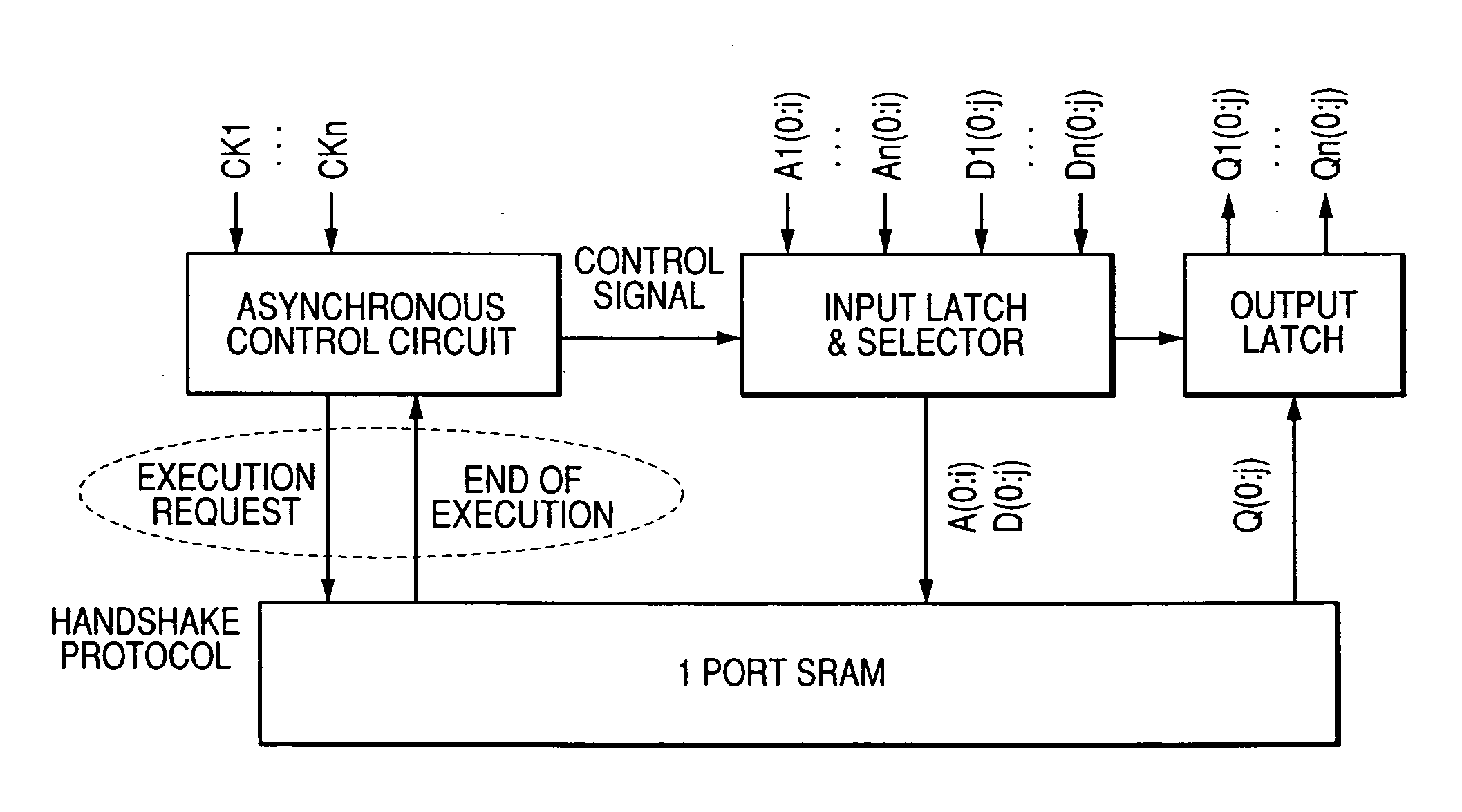
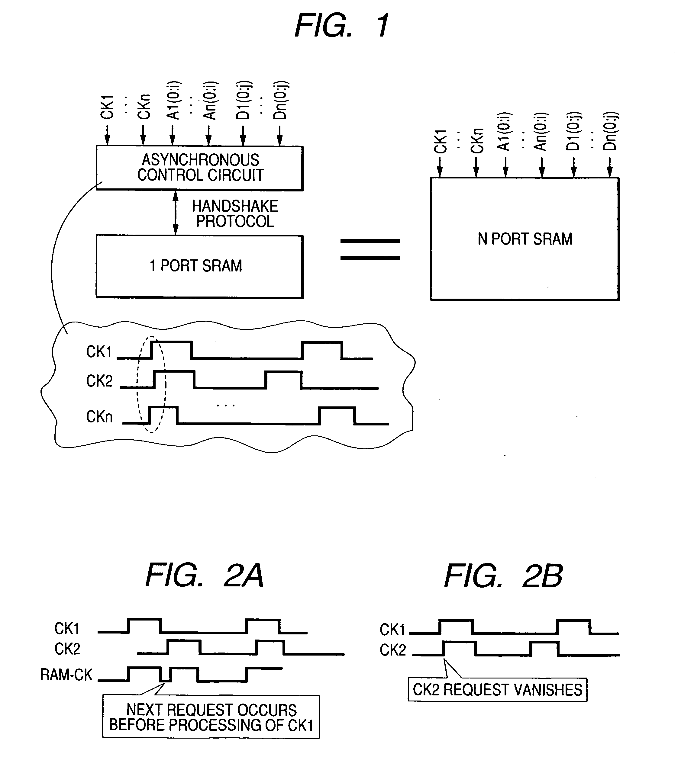
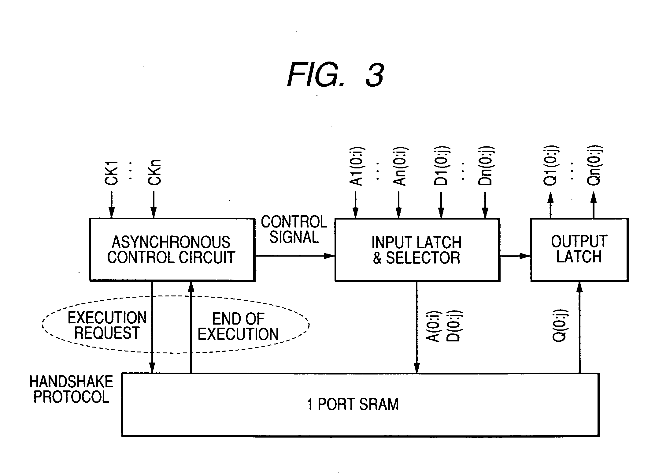
[0036]FIG. 1 is a concept diagram illustrating an example of an asynchronous type pseudo-multiport memory according to the present invention. The asynchronous type pseudo-multiport memory of this embodiment combines the asynchronous control circuit with a 1 port SRAM, achieving an equivalent N port SRAM. The above-mentioned asynchronous control circuit acknowledges the clock CK1-CKn, the address signal A1(0:i)-An(0:i) input according to each clock CK1-CKn, and the data signal D1(0:j)-Dn(0:j), and an equivalent N port SRAM is achieved by exchanging the signals with the 1 port SRAM according to a handshake protocol.

[0037] Here, the address signal (0:i) means i+1 bits from 0−i, and the data signal (0:j) means j+1 bits from 0−j. The above-mentioned clock CK1 or CKn is an access request signal when seen from the memory circuit side, for instance, a chip select signal CS and a chip enable signal CE are essentially regarded as the same as the above-mentioned clock CK in terms of circuit f...


PUM


Abstract

An asynchronous control circuit and a semiconductor integrated circuit achieving asynchronous operation and no limitation on the number of ports are offered. In an asynchronous control circuit, by being activated corresponding to at least one access request by acknowledging a plurality of access request signals generated asynchronously to each other and a plurality of input signals corresponding to each of the above-mentioned plurality of access requests, selecting one access request from one or more access requests in the activation mode, acknowledging an input signal corresponding thereto, transmitting the input signal to a memory, acknowledging the input signal corresponding to a non-executed access request after the end the operation corresponding to the input signal, and accessing the aforementioned memory circuit.

Description

CLAIM OF PRIORITY [0001] The present application claims priority from Japanese application JP 2003-272549 filed on Jul. 9, 2003, and Japanese application JP 2004-131238 filed on Apr. 27, 2004, the contents of which are hereby incorporated by reference into this application. FIELD OF INVENTION [0002] The present invention relates to an asynchronous control circuit and a semiconductor integrated circuit device and, for instance, to an effective method for use in circuit control technology accessing asynchronously a 1 port memory circuit from a plurality of ports. BACKGROUND OF THE INVENTION [0003] The area of a multi-port SRAM (static type random access memory) becomes very large compared to a 1 port SRAM because each port in the memory cell needs an access transistor, word line and bit line. Then, U.S. Pat. No. 6,625,686 (JP-A 57775 / 2000) proposed that a synchronous pseudo-multiport SRAM in which the function of an N port memory is artificially achieved by accessing the 1 port SRAM c...

Claims


Application Information

Patent Timeline
IPC IPC(8): G11C11/41G06F12/00G11C7/10G11C7/22H03K3/037
CPCG11C7/22G11C7/1075
Inventor NAKAHARA, SHIGERUHIGETA, KEIICHIKAWATA, TAKAHIRO
Owner HITACHI LTD
Why Eureka
Try Eureka