Switched-mode power amplifier using lumped element impedance inverter for parallel combining

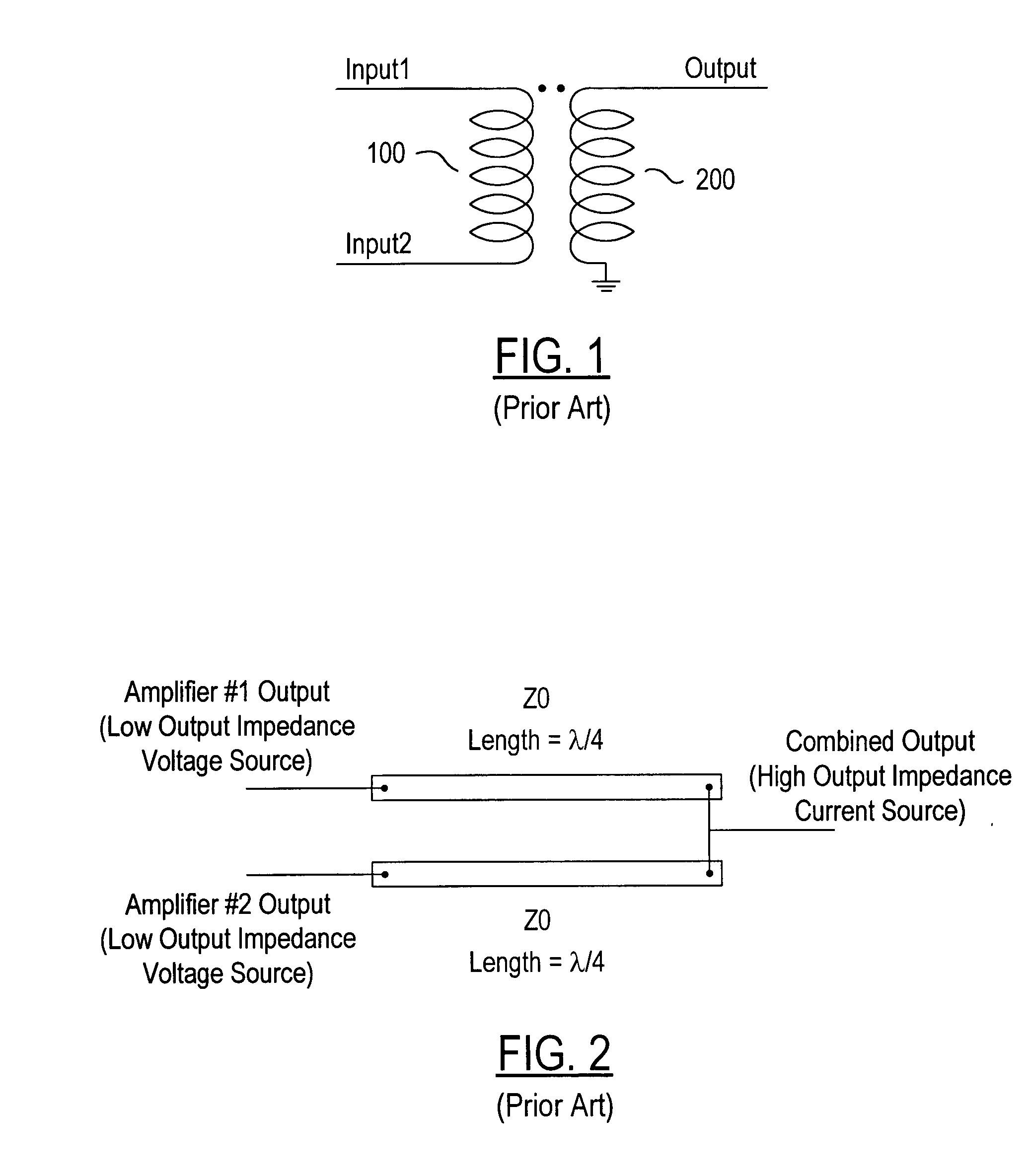
a technology of inverter and lumped element, applied in the field of circuitry, can solve the problems of insufficient isolation between the outputs of the two amplifiers of the appropriate combiner of the chireix-type amplifier, the inherent loss and isolation limitation, and the addition of difficulties in achieving efficiency at the amplification/combination stag

Inactive Publication Date: 2005-01-13
ZARBANA DIGITAL FUND
View PDF1 Cites 109 Cited by
  • Summary
  • Abstract
  • Description
  • Claims
  • Application Information

AI Technical Summary

Benefits of technology

[0014] In accordance with a further aspect of the invention there is provided a method for amplifying an input signal to produce an output signal configured for parallel connection with at least one other like output signal for combining the output signals within a Chireix circuit architecture. The input signal is amplified by means of at least one active device configured to be alternately switched by the input signal and an amplified signal corresponding to the input signal is presented, the amplified signal constituting a low output impedance voltage source. A second harmonic resonator configured for shorting a second harmonic signal of said input signal is provided across the active device. The low output impedance voltage source is transformed to constitute a high output impedance current source by means of a lumped element impedance inverter, the high output impedance current source being configured for the parallel connection. A third harmonic resonator blocks a third harmonic signal of the input signal from a load connected to the output signal. Negative reactive component values required by the impedance inverter are eliminated and effectively provided by incorporating those negative values into pre-selected adjacent reactive components of the resonators.

Problems solved by technology

Use of such independent modulated signals presents additional challenges to achieving efficiency at the amplification / combination stages of the transmitter, however, because the conventional model of amplification followed by combining, using known power amplifiers and combiners, is subject to inherent loss and isolation limitations.
Appropriate combiners for a Chireix-type amplifier do not provide any isolation between the outputs of the two amplifiers.
However, it will be understood by the skilled reader that such use of a magnetic transformer inherently introduces significant loss due to the limited Q achievable for the coils on a semiconductor substrate.
As will be appreciated by the skilled reader, these negative inductances, −L, can be realized, for a limited bandwidth (spot frequency) application, with the use of shunt capacitances; however, this is not applicable for a practical Class F amplifier for which such impedance inversion is needed at each of the first, second and third harmonics.
Consequently, the realization of such a transformation for Class F amplifier circuits presents an obstacle for the practical design and implementation of such a circuit.
However, it is also known that this Class F amplifier circuit architecture, where used at high frequencies, presents a design problem relating to the resonator circuits in that a source-drain (emitter-collector) parasitic capacitance results across the active device and causes the resonance values of these resonators to detune.

Method used


Image

  • Switched-mode power amplifier using lumped element impedance inverter for parallel combining
  • Switched-mode power amplifier using lumped element impedance inverter for parallel combining
  • Switched-mode power amplifier using lumped element impedance inverter for parallel combining

Examples


Embodiment Construction

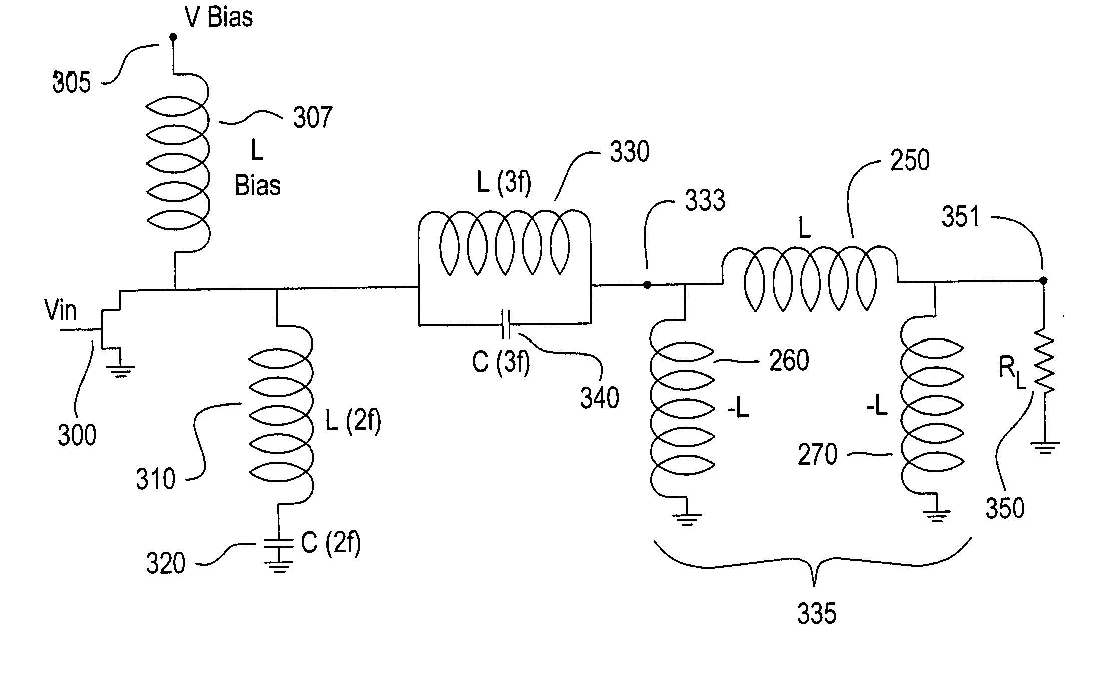
[0024] Surprisingly, the inventor has invented a Class F amplifier configured for parallel connection with at least one other like amplifier, for combining the outputs of such parallel connected amplifiers in a Chireix circuit architecture, which overcomes or avoids the disadvantages associated with the foregoing prior art transformer couplings used for combining amplifier outputs and impedance inverters in the form of quarter-wavelength transmission lines or lumped element equivalents thereto having negative reactive components.

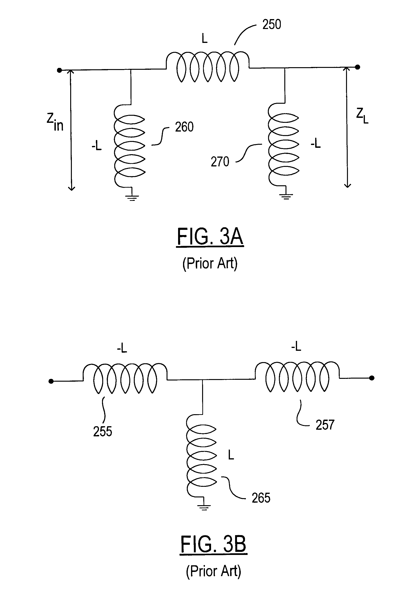
[0025] As illustrated by FIG. 5, the present invention is achieved by first transforming, by means of an impedance inverter 335 (consisting of series positive inductor 250 and shunt negative inductors 260, 270), the output of a Class F amplifier (i.e. at terminal 333) from that of a low impedance voltage source to a high impedance current source so that such output-transformed amplifier may be connected in parallel with another like amplifier configuration ...


PUM


Abstract

A switched-mode Class F power amplifier is provided for parallel connection with at least one other like amplifier, within a Chireix architecture, for combining the signals output therefrom. An input component includes at least one active device configured to be alternately switched by a signal input thereto to present an amplified signal corresponding to the input signal and constituting a low output impedance voltage source. A lumped element impedance inverter is provided between the input component and an output resonator component, the impedance inverter being configured for transforming the low output impedance voltage source to instead constitute a high output impedance current source configured for said parallel connection. In accordance with the invention, the negative reactive component values required by the impedance inverter are eliminated and effectively provided by incorporating those values into pre-selected reactive components of the input and output components. Further, a source-drain parasitic capacitance across the active device is eliminated by one or more pre-selected reactive components of the input component, the value(s) of which effectively compensate for the parasitic capacitance.

Description

FIELD OF THE INVENTION [0001] The invention relates to circuitry for radio frequency (i.e. “RF” or “wireless”) transmitters and, in particular, to a switched-mode power amplifier design and configuration for parallel connection with one or more like amplifiers for combining of the signals output therefrom. BACKGROUND OF THE INVENTION [0002] Typically, power combiners are used in RF transmitters to combine the output signals of parallel power amplifiers into one high power RF output signal for wireless transmission. In these known transmitter structures the signals are first amplified by the power amplifiers and then they are combined by a separate power combiner to produce a combined amplified signal for transmission. Depending upon the circuit architecture and signal format used, however, it becomes necessary to make trade-offs between reducing power losses and achieving isolation between input signals of the combiner. [0003] The need for efficiency is a particularly important desi...

Claims


Application Information

Patent Timeline
Patent Type & Authority Applications(United States)
IPC IPC(8): H03F1/56H03F3/217
CPCH03F1/0294H03F1/565H03F3/211H03F2200/402H03F3/68H03F2200/391H03F3/217
Inventor GRUNDLINGH, JOHAN M.
Owner ZARBANA DIGITAL FUND
Why Eureka
Try Eureka