Low voltage high gain amplifier circuits

a low-voltage, high-gain technology, applied in the field of amplifier circuits, can solve the problems of reducing the power supply voltage used in electronic systems, affecting the accuracy of amplifiers, and achieving higher gains in cascode circuits at the expense of headroom

Inactive Publication Date: 2005-01-13
ANALOG DEVICES INT UNLTD
View PDF1 Cites 12 Cited by
  • Summary
  • Abstract
  • Description
  • Claims
  • Application Information

AI Technical Summary

Problems solved by technology

However, in many actual implementations, the accuracy of an amplifier can be impaired by non-linearities in the open loop gain.
One trend in integrated circuit technology that has created challenges for amplifier circuit designers is the continuing reduction in the power supply voltages used in electronic systems.
However, cascode circuits achieve higher gains at the expense of headroom.
However, for optimum operation the maximum output voltage is limited as follows:
On the other hand, known cascode circuits are disadvantageous for low power supply applications because they have limited headroom.
This limited headroom can impact the ability of the circuit to amplify currents or voltages at the output or at intermediate nodes.
More particularly, at low power supply voltages, headroom limitations constrain the ability of cascode stages to drive inputs of transistors in an output stage across wide voltage ranges.
These limitations result in output stages that cannot provide accurate output voltages across wide voltage ranges.

Method used


Image

  • Low voltage high gain amplifier circuits
  • Low voltage high gain amplifier circuits
  • Low voltage high gain amplifier circuits

Examples


Embodiment Construction

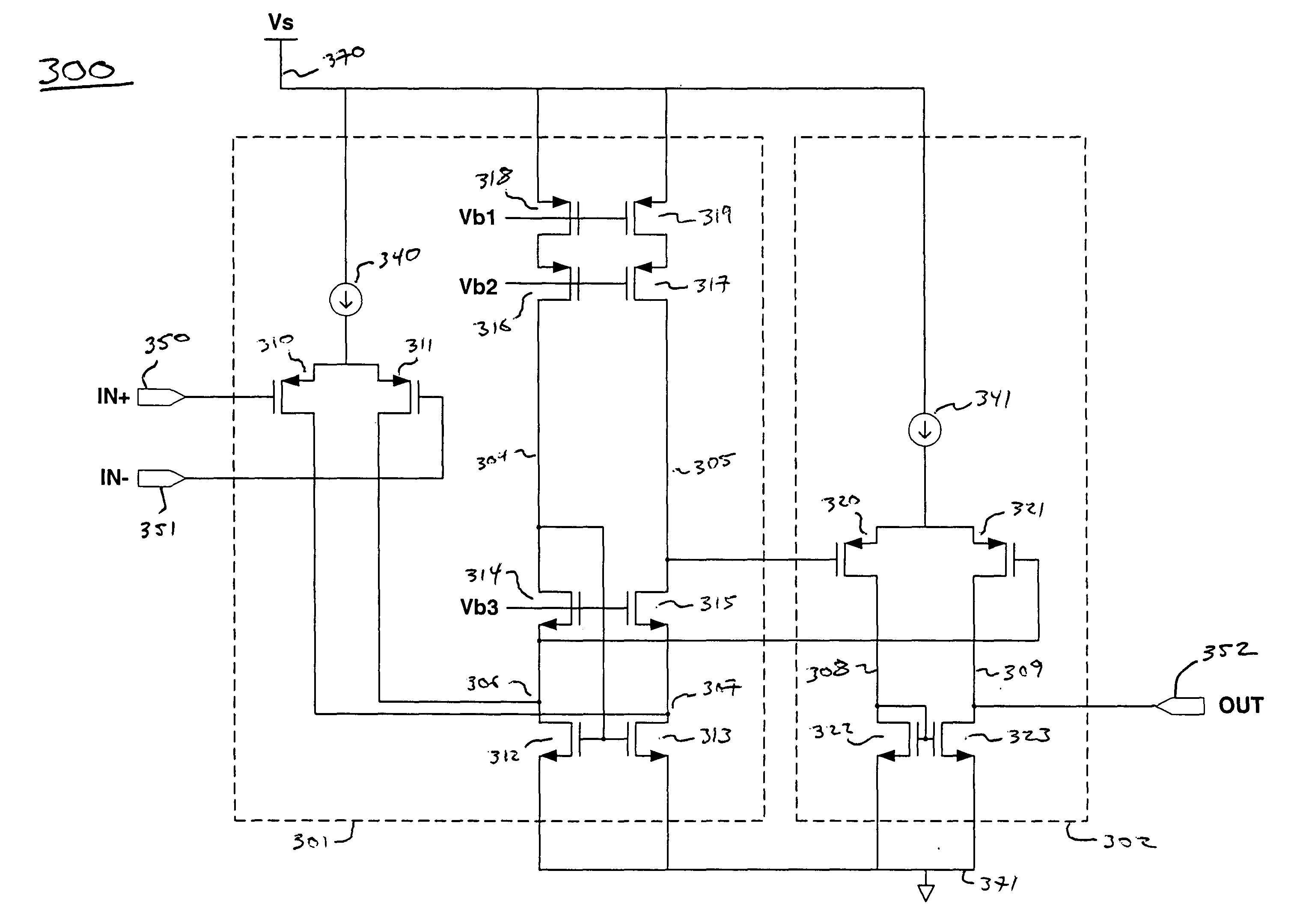
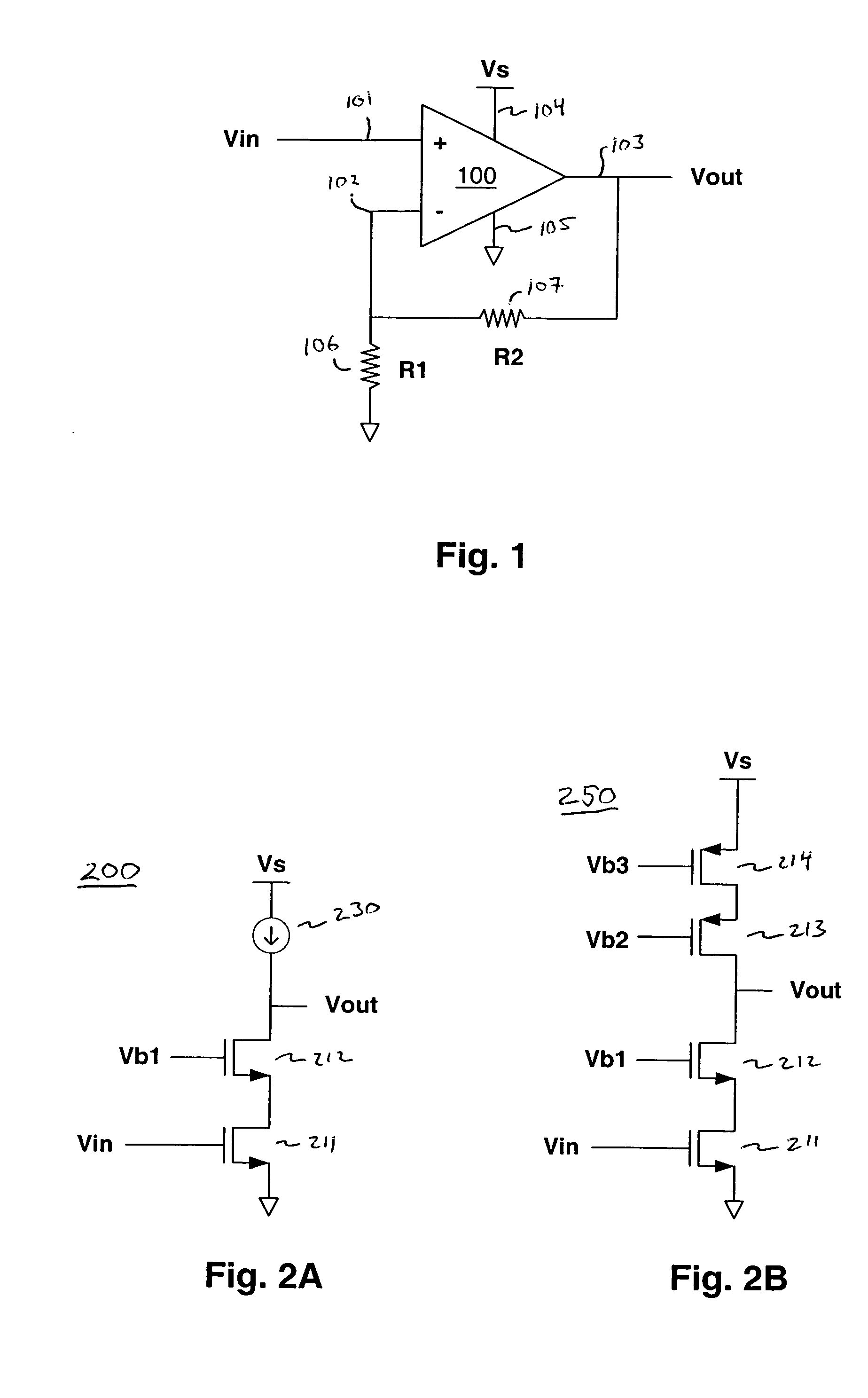
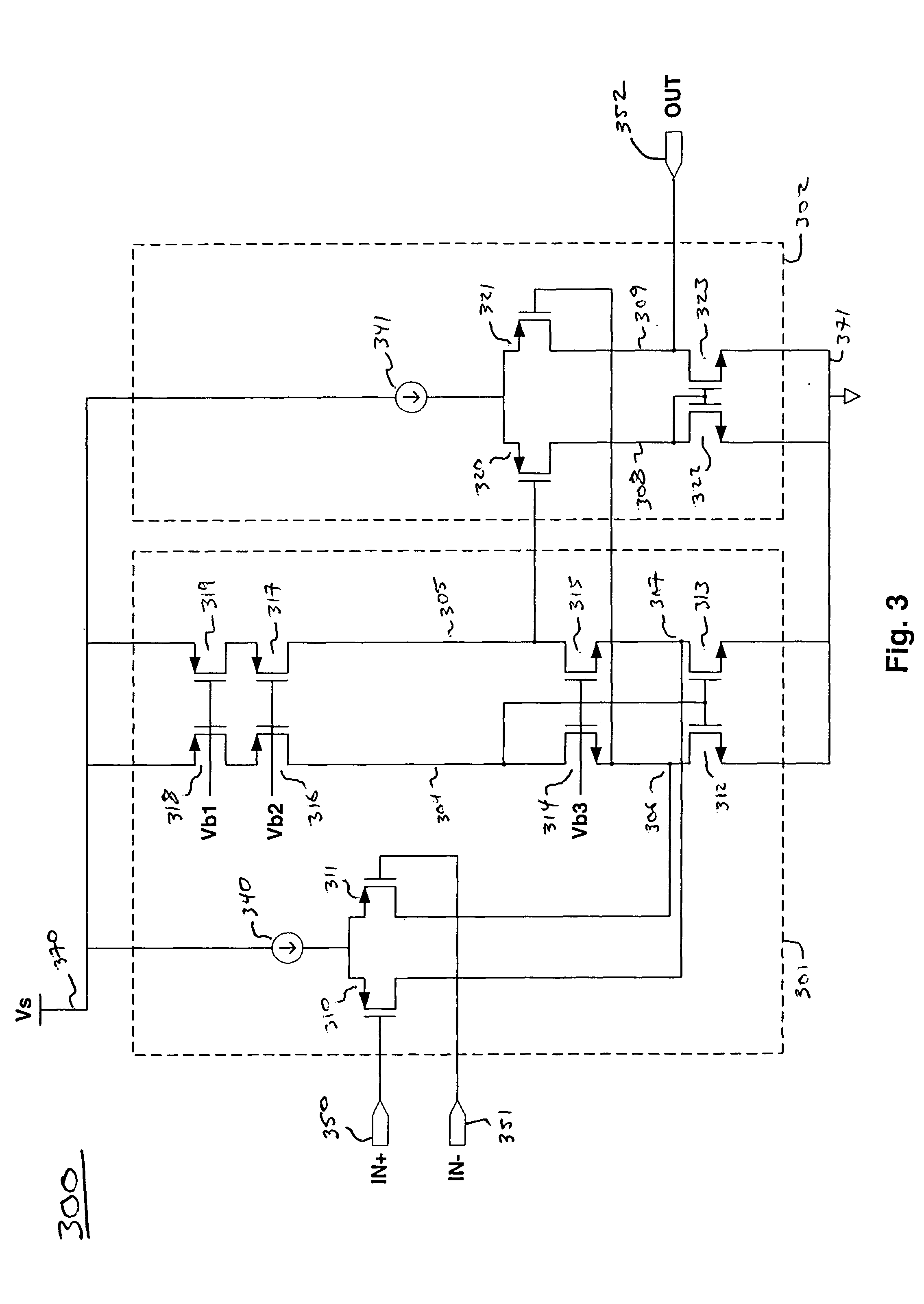
FIG. 3 illustrates two stages of an amplifier circuit 300 according to one embodiment of the present invention. Amplifier 300 includes a cascode input stage 301 and differential stage 302 implemented in a MOS technology. The MOS transistors shown include a gate control terminal, source terminal, and drain terminal. When the circuit is operating, supply voltages are applied to power supply terminals 370 and 371. Cascode input stage 301 includes input PMOS transistors 310 and 311. The gates of PMOS transistors 310 and 311 are coupled to input terminals 350“IN+”) and 351“IN−”), respectively. The sources of transistors 310 and 311 are both connected to a current source 340. Accordingly, when a differential voltage is applied across the input terminals, a differential current will be generated in the drain terminals of the PMOS transistors.

The drain of transistor 310 is coupled to cascode node 307 formed between cascaded transistor 313 and cascode transistor 315, and the drain of transi...


PUM


Abstract

In one embodiment, the present invention provides an amplifier circuit including a cascode input stage coupled to a differential stage. In another embodiment, an amplifier includes a differential stage coupled to a common gate stage. Embodiments of the present invention also include an improved low voltage amplifier using a 3-stage topology including a wide-swing folded-cascode input stage followed by a differential gain stage which provides improved gain and output compliance. Embodiments of the present invention improve the available cascode stage headroom and reject process and temperature induced parametric variations.

Description

BACKGROUND This invention relates to electronic circuits, and more particularly, to amplifier circuits useful in low power supply voltage applications. Amplifier circuits are used in a variety of electronic systems for increasing the voltage, current, or power of a signal. FIG. 1 shows one example of an amplifier 100 configured to receive an input voltage, Vin, and provide an amplified voltage, Vout. Amplifier 100 includes a positive input terminal 101“V+”), a negative input terminal 102“V−”), an output terminal 103 (“Vout”), a positive supply terminal 104, and a negative supply terminal 105. Input voltage, Vin, is received on terminal 101, and the amplified voltage, Vout, is provided on terminal 103. Amplifier 100 includes feedback resistors 106“R1”) and 107“R2”), which are connected in a “closed loop” to provide negative feedback. The output voltage, Vout, of amplifier 100 is related to the inputs according to the following well-known equation:Vo=G(V+−V−), where “G” is the “open...

Claims


Application Information

Patent Timeline
Patent Type & Authority Applications(United States)
IPC IPC(8): H03F3/30H03F3/45
CPCH03F3/3023H03F3/303H03F2203/45651H03F2203/45028H03F3/45192
Inventor SCHRADER, VICTOR PAUL
Owner ANALOG DEVICES INT UNLTD
Why Eureka
Try Eureka