Solution-processed thin film transistor formation method

a thin film transistor and formation method technology, applied in semiconductor devices, solid-state devices, electrical devices, etc., can solve the problems of large feature size, complexity and expense, and add complexity and expense, which contradict the goal of achieving simple manufactured devices and circuits, and small gaps

Inactive Publication Date: 2005-01-13
HEWLETT PACKARD DEV CO LP
View PDF15 Cites 55 Cited by
  • Summary
  • Abstract
  • Description
  • Claims
  • Application Information

AI Technical Summary

Benefits of technology

[0005] An exemplary solution-processed thin film transistor formation method of the invention forms conductive solution-processed thin film contacts, semiconductor solution-processed thin film active regions, and dielectric solution-processed thin film isolations in a sequence and organization to form a solution-processed thin film structure capable of transisto

Problems solved by technology

A critical issue, however, remains feature size.
However, introducing conventional techniques to produce small feature sizes, e.g., lithography, adds complexity and expense that contradi

Method used


Image

  • Solution-processed thin film transistor formation method
  • Solution-processed thin film transistor formation method
  • Solution-processed thin film transistor formation method

Examples


Embodiment Construction

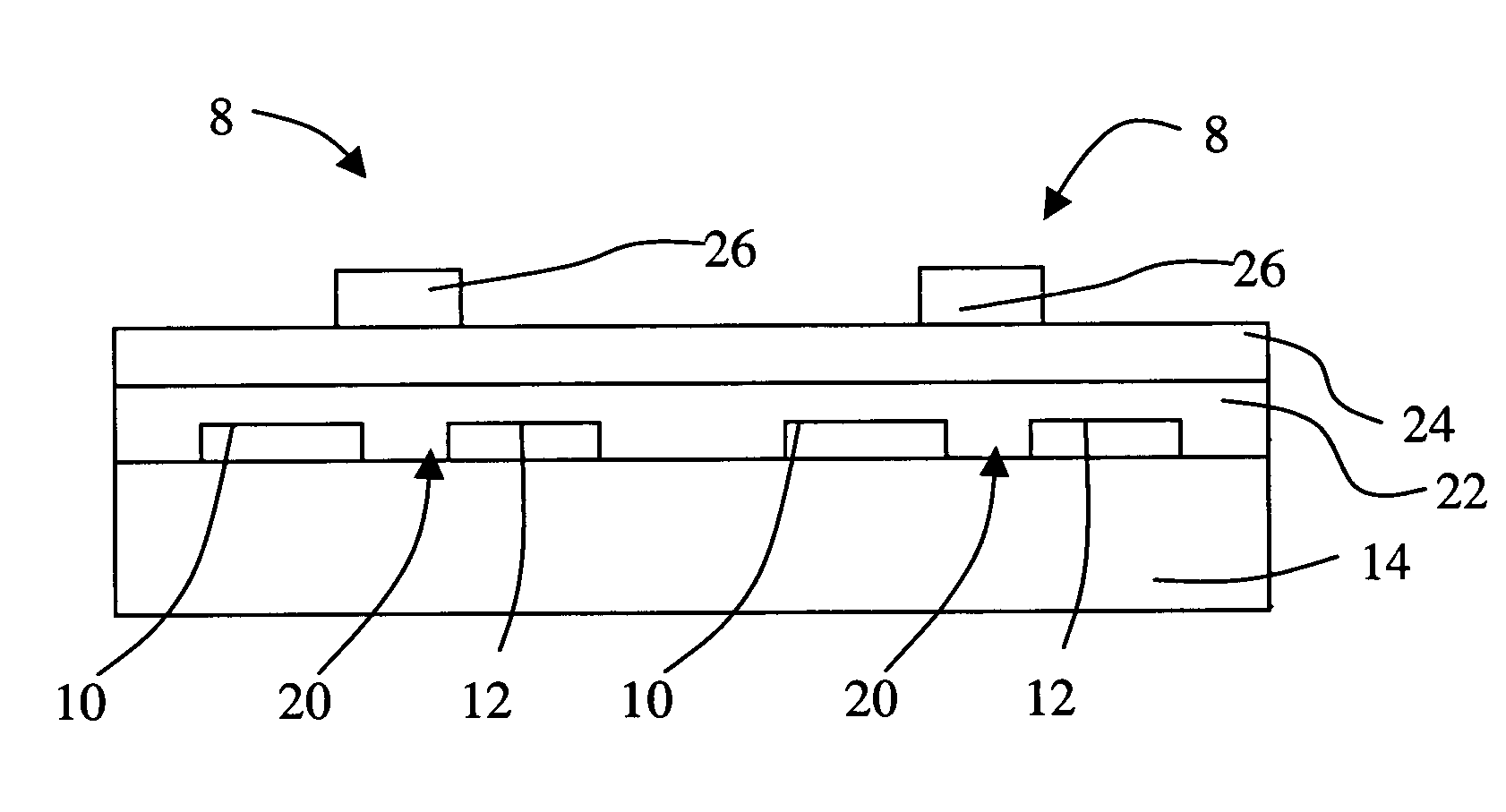
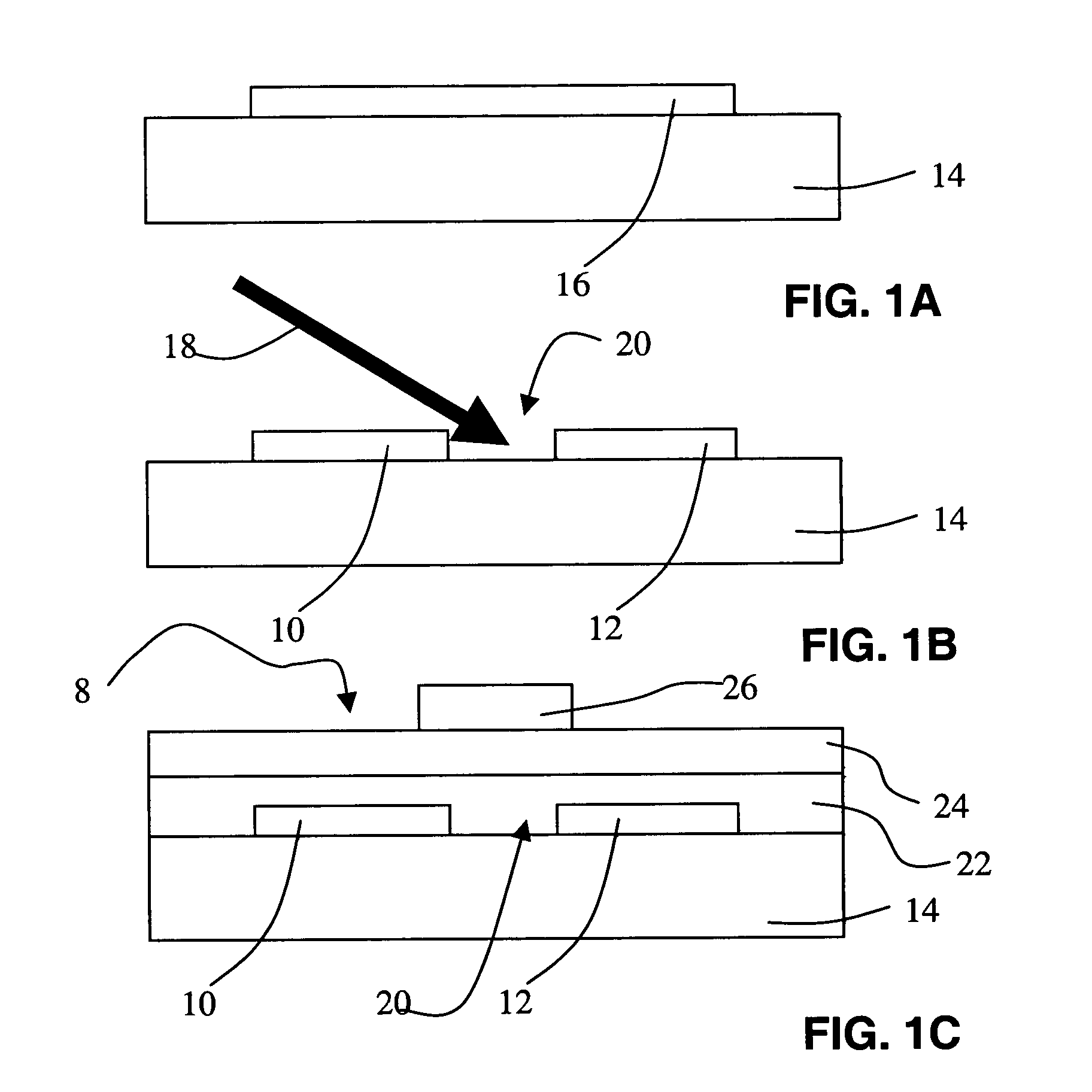
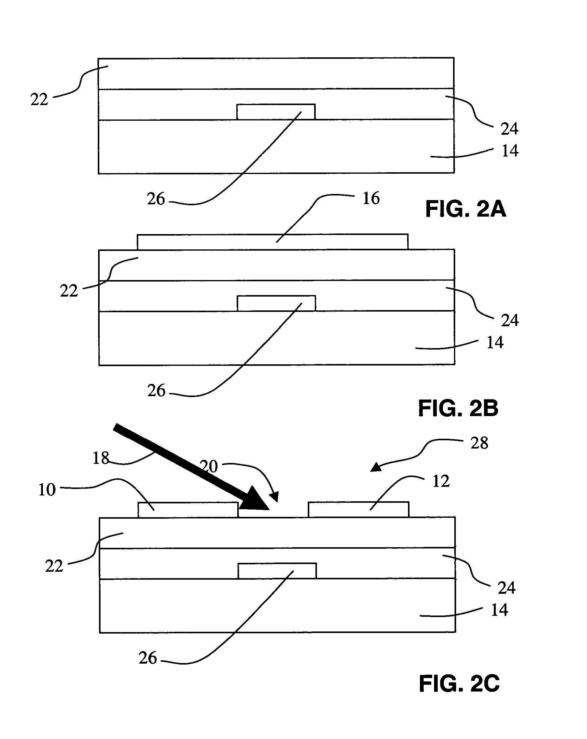
[0011] The invention concerns solution-processed thin film transistor formation that makes use of selective laser ablation to remove material as part of a patterning step. Solution-processed, as applied to modify material and thin film and used herein, refers to those materials that are either soluble in a solution or capable of suspension in a solution so they may be processed by a solution technique, e.g., ink jet printing or spin coating, and formed into a thin film. Exemplary categories of solution-processed thin films include organic thin films and polymer thin film categories. The majority of the solution-processed materials that can be formed into thin films are the conductive polymers, semiconductive polymers and dielectric polymers. However, a solution-processed material may also be a precursor of small organic molecular material that is soluble in a solvent. One example is the pentacene precursor that is soluble in chloroform. It can be spin-coated to form a thin film and ...


PUM

PropertyMeasurementUnit
Lengthaaaaaaaaaa
Electrical conductoraaaaaaaaaa
Wavelengthaaaaaaaaaa

Abstract

An exemplary solution-processed thin film transistor formation method of the invention forms conductive solution-processed thin film material contacts, semiconductor solution-processed thin film material active regions, and dielectric solution-processed thin film material isolations in a sequence and organization to form a solution-processed thin film structure capable of transistor operation. During or after the formation of the transistor structure, laser ablation is applied to one or more of the conductive solution-processed thin film material contacts, the semiconductor solution-processed thin film material active regions and the dielectric solution-processed thin film material isolations to pattern or complete patterning of a material being selectively ablated.

Description

FIELD OF THE INVENTION [0001] The invention is in the semiconductor field. The invention particularly concerns solution-processed thin film transistors. BACKGROUND OF THE INVENTION [0002] Solution-processed thin film transistors hold great promise to fundamentally change the semiconductor industry. Solution-processed, as applied to modify material and thin film and used herein, refers to those materials that are either soluble in a solution or capable of suspension in a solution so they may be processed by a solution technique, e.g., ink jet printing or spin coating, and formed into a thin film. Their uses run the gamut of conventional transistor uses, and may be formed into light emitting structures. Materials used in the thin films, such as conductive polymers, are durable and can be flexible, thereby providing a range of uses in demanding environments. [0003] The solution-processed thin film transistors also hold the potential to be fabricated by simple techniques, e.g., direct p...

Claims


Application Information

Patent Timeline
IPC IPC(8): H01L21/336H01L51/00H01L51/05H01L51/30H01L51/40
CPCH01L27/283H01L29/66742H01L51/0017H01L51/0021H01L51/0545H01L51/0037H01L51/0097H01L51/0541H01L51/0036H10K19/10H10K71/231H10K71/60H10K85/113H10K85/1135H10K10/464H10K10/466H10K77/111
Inventor WENG, JIAN-GANGPRASAD, RAVIADDINGTON, CARY G.CHEUNG, MAN HO
Owner HEWLETT PACKARD DEV CO LP
Why Eureka
Try Eureka