Method of forming thin film patterning substrate including formation of banks

a technology of thin film patterning and substrate, applied in the direction of identification means, instruments, transportation and packaging, etc., can solve the problems of large volume of liquid material deployed in the enclosed area of the partitioning member, large volume of liquid material deployed in the area after film fabrication, and large volume of liquid material deployed in the enclosed area. , to achieve the effect of fine and highly detailed patterning, high precision and good yield

Inactive Publication Date: 2005-08-25
SEIKO EPSON CORP
View PDF6 Cites 96 Cited by
  • Summary
  • Abstract
  • Description
  • Claims
  • Application Information

AI Technical Summary

Benefits of technology

[0027] It is in the face of these circumstances that the present invention was arrived at. The primary objects of the present invention are, when forming film patterns using thin films of different properties on the same substrate, to prevent liquid thin film materials from flowing over the banks, to be able to form thin film layers that are flat and of uniform thickness with no color irregularities, without fail, with high precision, relatively simply, and with good yield, and to make possible very fine and highly detailed patterning.

Problems solved by technology

When an ink jet process is used, however, a problem arises at the process surface in that the different thin film materials become mixed on the substrate.
This presents a problem.
In recent functional devices, and particularly in display elements, thinness is generally demanded, and, despite the fact that this places limitations on the height of the partitioning members, the volume of liquid material deployed in the areas enclosed by the partitioning members is far greater than the volume remaining after film fabrication.
For this reason, problems arise in terms of poor balance between the size of the liquid droplets discharged into the areas enclosed by the partitioning members and the surface areas both of the partitioning member surfaces and of the areas enclosed therein.
In cases where the partitioning members exhibit liquid affinity or wettability relative to the liquid material that is the thin film material to be deployed, the desired film thickness cannot be obtained in the final thin film even when partitioning members are present since [the liquid material] is pulled by the partitioning members.
If that is not the case, the liquid material will not wet and spread over the areas enclosed by the partitioning members, and, with display elements such as EL devices, in particular, color loss and color irregularity will develop in the pixels.
However, even when water repellency in the upper surfaces of the partitioning members and liquid affinity in the areas enclosed by the partitioning members are to some degree realized, in cases where the liquid material is applied using an ink jet process, for example, if the size of the liquid droplets discharged is extremely large or small relative to the surface area of the surfaces of the partitioning members noted above or of the areas enclosed thereby, or if the balance therebetween is otherwise very poor, it is known that the liquid material is not accurately deployed in the areas coated, so that high-precision patterning becomes impossible.
In cases such as this, when there is an unsuitable relationship between liquid droplet size and the surface area of the areas enclosed by the partitioning members, what happens is that, due to the problems noted earlier, liquid thin film materials become mixed together in the areas enclosed by the partitioning members, and film thickness variation develops in each thin film that is formed.
Problems also arise which relate to the affinity of the partitioning members toward the liquid thin film material when that thin film material is deployed in the areas demarcated by the partitioning members.
Nevertheless, when member surfaces are made ink-repellent using a fluorine compound or members are formed using a fluorine compound material, in particular, the bonding strength between the fluorine-based material and the underlying layer or underlying substrate forming the members becomes poor, which presents problems in terms of applications to bank-forming technology.
Even if the members, and particularly the banks themselves, are formed with an ink-repellent fluorine compound material or the like, residue develops in the bank areas after patterning by photolithography, whereupon there is a danger of the ink affinity of the bank surfaces being impaired.
There has been a tendency for a slight affinity to develop due to UV irradiation, even when the material is one exhibiting non-affinity, thereby negating the effectiveness of the non-affinity treatment.
This results in color irregularities in the pixels in the display elements.
In EL devices, in particular, shorts readily develop, leading to reduced reliability.
Nevertheless, because most of the liquid of the thin film material is pulled to the side surfaces of the partitioning members, not only does the film thickness become greater in the lower skirt portion of the thin film, that is, in the portions in contact with the substrate, but neither is it difficult to control the film thickness.
No technology has been reported, however, for simply and rigorously controlling the wettability of each material in the substrate by plasma treatment or UV irradiation in cases where a pattern of layers constituted by organic or inorganic substances is formed on the same substrate.
With methods wherein ink repellency is imparted by mixture-gas plasma treatment to an organic substance surface or the surface of a member formed of an organic substance, problems arise, such as being unable to impart ink repellency efficiently, or that the ink repellency of the surface is transient, or having to use a heat treatment, so that the ink repellency deteriorates with the passage of time.
In cases where an ink-affinity treatment is performed using energy irradiation, there is a danger of impairing the ink repellency of the bank surfaces, and it is very difficult to simultaneously achieve both bank surface ink repellency and bank surface ink affinity.
When this happens, it is not possible to form thin films having the desired characteristics.
If the depressions do not exhibit ink affinity, the wetting and spreading within the pixels will be poor, causing color loss and film thickness irregularity.
Thus these methods involve difficulties in that controlling the ink supplied is difficult and in that the number of process steps becomes large.

Method used


Image

  • Method of forming thin film patterning substrate including formation of banks
  • Method of forming thin film patterning substrate including formation of banks
  • Method of forming thin film patterning substrate including formation of banks

Examples


first embodiment (

(1) First Embodiment (Aspect Employing Ink Jet Method)

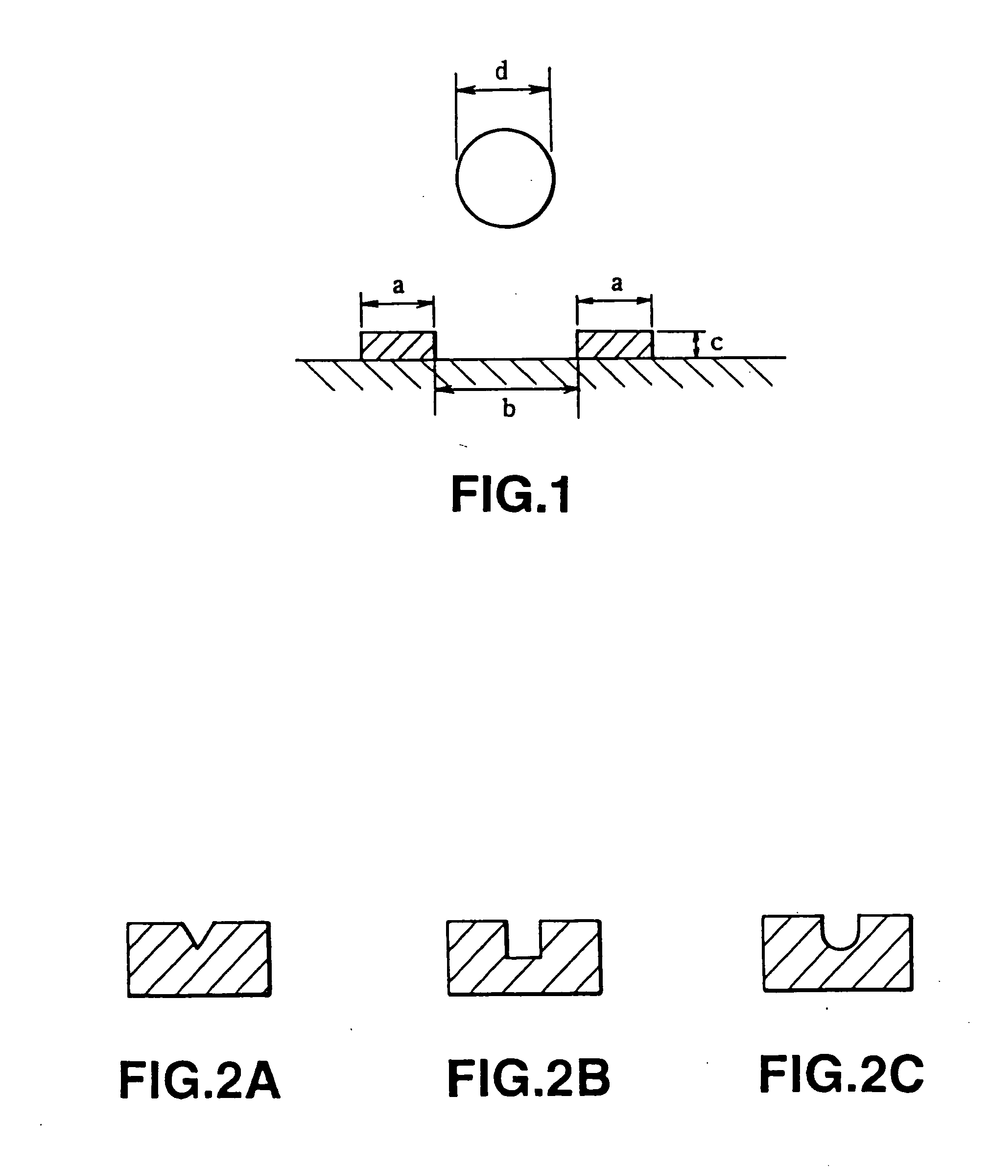
[0100] In a display device having, on a substrate, banks of a prescribed height, and a thin film layer formed by an ink jet method on the surface of the substrate divided by those banks, when the width of the banks is made a (μm), the height thereof is made c (μm), the width of the areas to be coated, divided by the banks, is made b (μm), and the diameter of the liquid droplets of the liquid material forming the thin film layer is made d (μm), the banks are formed on the substrate so as to satisfy the relationships a>d / 4, d / 2t0 (where t0 is the film thickness of the thin film layer in μm), and c>1 / 2×d / b.

[0101]FIG. 1 is a model diagram for describing the relationship between the liquid droplets and the banks provided on the substrate when the display device of the present invention is formed by an ink jet method.

[0102] (a) Bank Configuration

[0103] The banks (also called risers or partitioning members) provided on the substrate ...

second embodiment (

(2) Second Embodiment (Aspect Employing Dipping or Spin-Coating Method)

[0123] The inventors discovered that, in a display device having a thin film layer formed by a dipping or spin-coating method, wherein banks of a prescribed height and areas to be coated partitioned by those banks are provided on a substrate, and surface treatment is performed as desired, the objects of the present invention can be achieved even with a thin film formation method characterized by the fact that the thin film layer is formed using a liquid material having a surface tension of 30 dyne / cm. In particular, with the display device described above, unlike in cases where coating is done using an ink jet process, the objects mentioned can be achieved by controlling the surface energy of the liquid material in addition to the surface energy of the banks and substrate, without imposing any limitation whatever on the shape or size of the banks or areas to be coated. It is therewith possible, furthermore, to ef...

specific embodiment aspect

(3) Third Embodiment (Specific Embodiment Aspect of Display Device)

[0125] (Configuration)

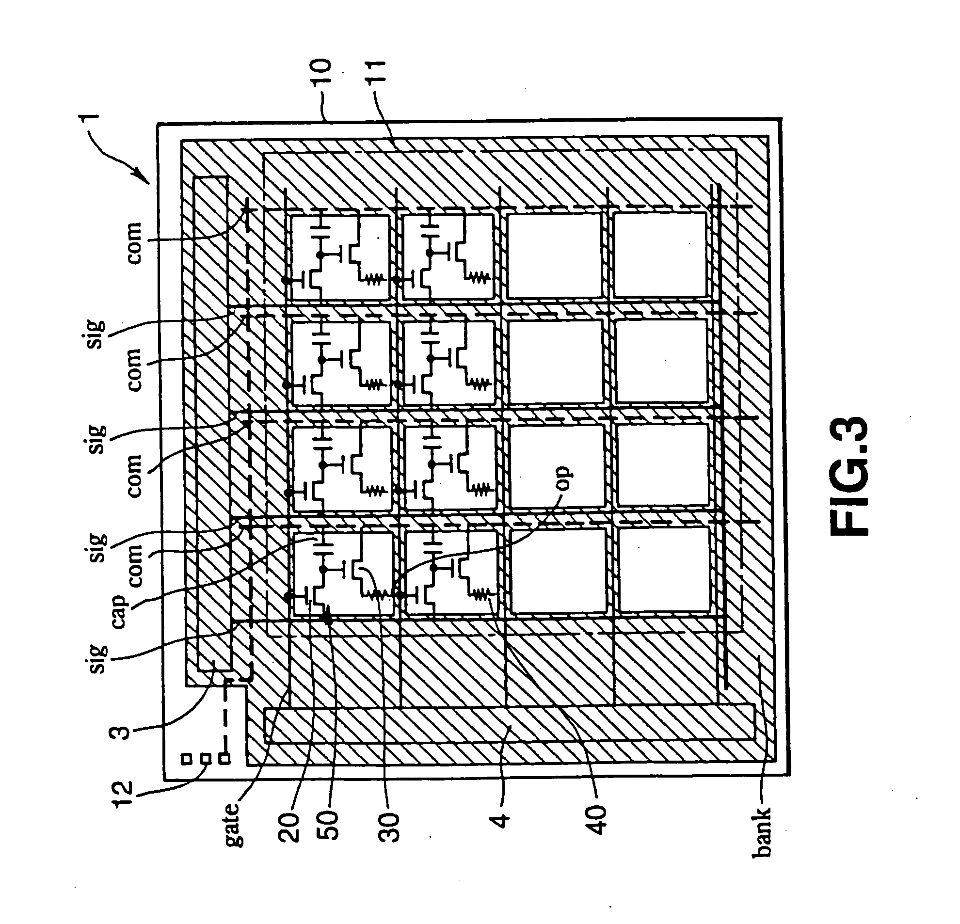
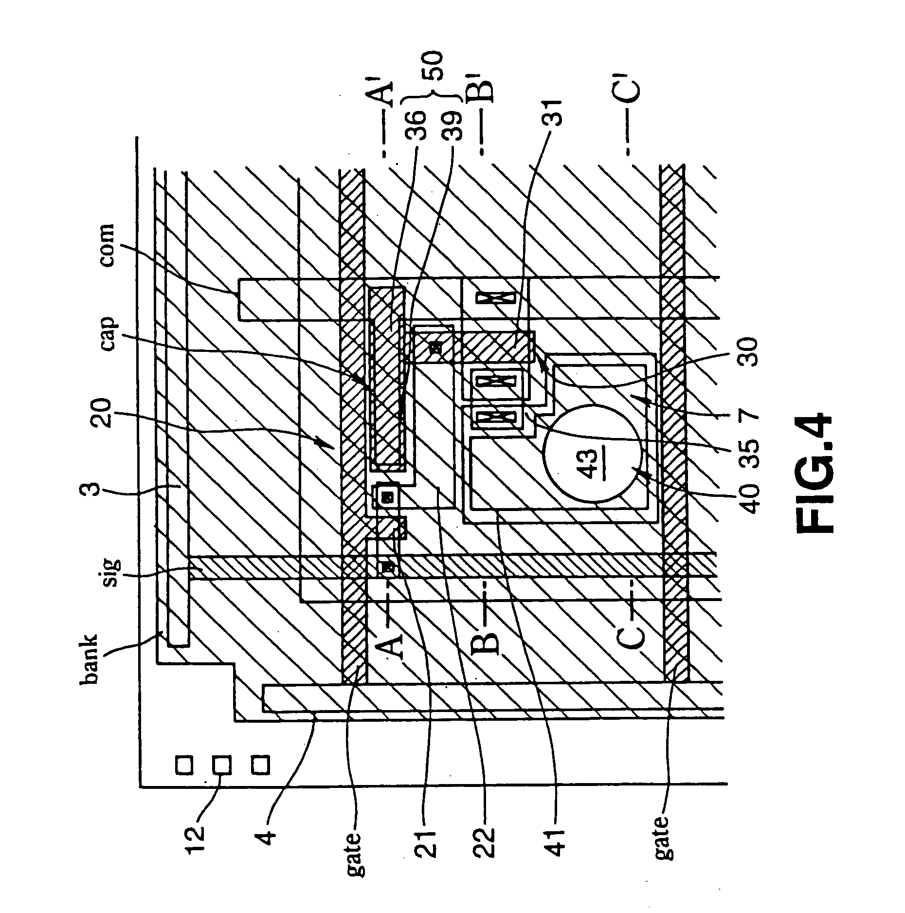
[0126]FIG. 3 is a model block diagram of the overall layout of an active-matrix type display device in this embodiment aspect. FIG. 4 is a plan of one pixel in FIG. 3, and FIG. 5A-5C are cross-sections in the A-A plane, B-B plane, and C-C plane, respectively, in FIG. 4.

[0127] The active-matrix type display device of this embodying aspect comprises a display unit 11 in the center portion of a transparent substrate 10. In the peripheral portion of the transparent substrate 10 is provided a data-side drive circuit 3 and a scanning-side drive circuit 4. Data lines SIG are wired to the display unit 11 from the data side drive circuit 3, and scanning lines GATE are wired from the scanning side drive circuit 4. In these drive circuits 3 and 4 are configured complimentary TFTs by an N-type TFT and a P-type TFT (not shown). These complementary TFTs configure shift register circuits, level shifter circu...


PUM

PropertyMeasurementUnit
angle of contactaaaaaaaaaa

Abstract

Display devices such as EL elements or LED elements, are formed from thin film elements having banks of prescribed height and a thin film layer formed by an ink jet method in areas to be coated that are partitioned by those banks. The banks may be formed of an organic material on a bank formation surface configured of an inorganic material, plasma treatment is performed under conditions that the induction gas is fluorine-based and that fluorine is present excessively, and the areas enclosed by the banks subjected to surface treatment are filled with the liquid thin film material to form the thin film layer or layers.

Description

TECHNICAL FIELD [0001] This invention relates to thin film formation technology suitable for manufacturing color filters or display elements such as LEDs (light emitting diodes) or EL (electro-luminescence) devices which use organic semiconductor films. [0002] More particularly, the present invention relates to substrates, a thin film formation method, and thin film elements used in forming patterns on substrates when thin films having different properties are formed on the same substrate. The present invention also relates to a method of forming thin films on which fine patterning is required, wherewith it is both easy to form thin film layers using an ink jet process and possible to form flat thin film layers. The present invention further relates to a surface modification method for performing superfine patterning wherewith a liquid thin film material is deployed in areas enclosed in banks formed on a substrate, using an ink jet method or spin coating, etc., as well as to a metho...

Claims


Application Information

Patent Timeline
Patent Type & Authority Applications(United States)
IPC IPC(8): G02B5/20G09F9/00G09F9/30G09F9/33H01L27/32H01L33/26H01L33/42H01L33/48H01L51/00H01L51/40H01L51/50H01L51/52H01L51/56H05B33/10H05B33/12H05B33/14H05B33/22
CPCG02B5/201H01L27/322H01L27/3246H01L51/0005Y10T428/24802H01L51/5284H01L2251/558H05B33/10H05B33/22H01L51/0014H10K59/38H10K59/122H10K71/135H10K71/20H10K2102/351H10K59/8792H10K50/865
Inventor SEKI, SHUNICHIKIGUCHI, HIROSHIYUDASAKA, ICHIOMIYAJIMA, HIROO
Owner SEIKO EPSON CORP
Why Eureka
Try Eureka